- Home
- Users & Science
- Scientific Documentation
- ESRF Highlights
- ESRF Highlights 2010
- Structure of materials
- Self-assembly of porphyrins on a single crystalline organic substrate
Self-assembly of porphyrins on a single crystalline organic substrate
The crystallinity of a material is of great importance for electronic applications. This holds true especially for poorly conducting materials, which are used in, for example, organic electronics. For practical use, these materials need to be deposited on a surface, preferably in crystalline form. Better crystal quality with large domains can increase properties like conductivity by more than one order of magnitude. Control over the crystal growth direction is highly desirable, because, if only one growth direction is present, different domains will coalesce to form one single crystalline layer. Growth on single crystalline substrates can be used to control the direction of growth. A low-symmetry crystal substrate will induce fewer growth directions for the grown material and thus leads to better crystal quality. Inorganic substrates are the most commonly used substrates, but they are generally of high symmetry.
In our study we used potassium acid phthalate (KAP) as an organic substrate with low symmetry. It has an ionic structure, but the cleaved surface consists of apolar benzene rings. Because of π-π interactions, this surface provides an interesting template for the layer growth of many kinds of aromatic molecules. A purely organic porphyrin with C11 tails was grown from heptane on these KAP substrates by drop deposition and evaporation; an n-heptane layer was also studied for the purpose of comparison.
 |
|
Fig. 32: Specular reflectivity curves of KAP with pure n-heptane film (filled circles) and with a porphyrin solution film (open circles), where Fhkl is the structure factor and k is the diffraction index perpendicular to the surface. The only noticeable difference is in the first fringes, which are caused by the film thickness. The solid curve is a fit of (010) KAP covered by a disordered monolayer of C atoms, representing the n-heptane solution. The dashed line is a fit of the (010) KAP substrate surface without this layer. |
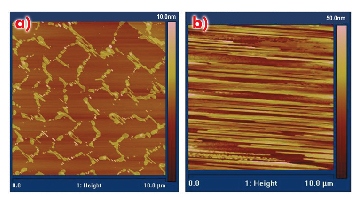
To grow ordered layers we used a wide range of solute concentrations going from undersaturated to supersaturated, which results in a large variety of different layer structures. These structures were studied with the complementary techniques of atomic force microscopy (AFM) and surface X-ray diffraction (SXRD) at ID03 and BM26/DUBBLE. The surface of the underlying substrate was first characterised and shown to be bulk terminated using SXRD. In situ measurements of the growth solutions on the surface show the thickness of the solution film and the presence of out-of-plane ordering (‘layering’), see Figure 32. However, the in-plane ordering could not be seen, probably, because of radiation damage. Ex situ these structures were studied by AFM and we found that round islands are formed at the KAP surface at the lowest concentration of porphyrin solution. At somewhat higher concentrations, but still undersaturated, we enter the self-assembly regime. Here the islands show one preferred growth direction (Figure 33a) and grow together to form mono and multilayer structures. The step height of these structures is 2.5 nm, which corresponds to the planar porphyrin molecules lying perpendicular to the substrate surface. At higher concentrations, corresponding to a supersaturated solution, another stacked formation was found when more than 5 multilayers are formed. At these higher concentrations, the growth was no longer layer-wise, but nano-needles were formed, shown in Figure 33b.
 |
|
Fig. 33: AFM images of a) a honeycomb structure composed of oriented islands, b) nano-needle structure. The orientation of the porphyrin molecules in the nano-needles is determined via X-ray diffraction. |
These nano-needles are oriented in the same direction, forming a single crystalline needle layer on the KAP surface. The molecular ordering in the nano-needles differs from that in the mono and multilayers. From the lattice spacing of 0.9 nm, as determined from X-ray diffraction, it follows that here the molecules are stacked in a tilted fashion, inclined by approximately 45 degrees. Both structures, the (multi)layers and the nano-needles, are oriented in one crystallographic direction over the whole substrate, which can reach an area of up to 1 cm2. By using alternative organic crystals as substrates, the assembly can in principle be tuned to give organic crystal layers with unique electronic or photophysical properties.
Principal publication and authors
F.J. van den Bruele, J.A.A.W. Elemans, A.E. Rowan, W.J.P. van Enckevort and E. Vlieg, Langmuir 26, 498-503 (2010).
Radboud University Nijmegen, Institute for Molecules and Materials (IMM) (The Netherlands)
partners


European Synchrotron Radiation Facility - 71, avenue des Martyrs, CS 40220, 38043 Grenoble Cedex 9, France.