- Home
- News
- General News
- Nanoparticles to...
Nanoparticles to make nanostructures function: a game of hide and seek?
21-02-2022
Scientists from the University of Twente in The Netherlands and the European Synchrotron Radiation Facility (ESRF) in France have devised new methods to place nano-emitters inside 3D photonic nanostructures. The results, which could open doors to make microchips much smaller, are published today in ACS Nano.
Nanoparticles, inserted in the form of quantum dots in nanostructures, can make these nanostructures develop specific functions, notably in efficient miniature lasers and light-emitting diodes, photovoltaics, electric capacitors, gas sensors, energy conversion and batteries.
Until today, scientists would place the nanoparticles inside randomly but would not know where exactly in the nanostructure they were. However, the performance of these 3D functionalised nanostructures depends on the precise positioning of the nanoparticles. In nanophotonics, for instance, fluorescing nanoparticles should reside at positions where the light field is maximal, such as in cavities or near an antenna. In biochemical detectors, antibodies should be positioned on the internal interfaces of the 3D substrate for maximum reactivity and selectivity.
Scientists from the University of Twente and the ESRF have found new methods to place (“hide”) nano-emitters inside 3D photonic nanostructures made of silicon and to be able to locate them (“seek”) afterwards using synchrotron X-ray nanofluorescence. “It is the first time that we can actually acquire a complete element-specific image of the internal device structure without damaging it, therefore allowing us to further use and test the devices”, explains Willem Vos, professor at the University of Twente and corresponding author of the article.
In their research, the scientists created 3D photonic crystal devices from silicon with a diamond-like structure that consists of two perpendicular sets of nanopores. They then infiltrated quantum dot nanoparticles, which were attached to polymer brushes that grew from the nanopore walls.
Even more challenging than the infiltration (“hide”) was the characterisation of the infiltrated nanostructure (“seek"). Andreas Schulz, researcher at the University of Twente and first author of the publication, explains: “The preparation process of inserting nanometre-sized quantum dots is actually quite complex and nanotechnological processes often present surprises, which means that the nanoparticles can easily end up in the wrong place!” It is therefore critical to assess the structure of a 3D nanomaterial and verify the position of certain key-elements.
In order not to damage the device, the team turned onto an original methodology in nanotechnology: element-specific synchrotron X-ray fluorescence tomography (SXRF), in order to non-destructively assess the functionalized nanostructures. “The experiment was quite tough, not only for the duration (it took 40 hours for just one sample) but also for the complex data that it generated and that we had to analyse afterwards”, explains Peter Cloetens, scientist in charge of ESRF’s ID16A.
In their X-ray experiments at ESRF’s ID16A, the team focused an X-ray beam onto the sample with quantum dots. They then detected secondary X-rays emitted by the sample, while both rotating and translating the sample’s position. The involved elements are identified from the known X-ray emission spectra, combined with the chemical compounds known from the sample preparation. They detected silicon (from the substrate), chlorine and copper from the involved catalyst (Cl also from the polymer brushes), and chromium and gallium as a trace element from the creation. Lead is the signature of the infiltrated lead sulfide (PbS) quantum dots. The results led the team to the conclusion that the quantum dots have indeed been successfully infiltrated into the nanopores of the 3D photonic crystal. Vos explains the added value of the ESRF: “The outcome of the experiment clearly shows that the X-ray fluorescence tomography set-up at the ESRF is a very powerful tool to characterise functional nanoparticles in complex 3D architectures."
On top of the location of the quantum dots, the researchers also observed that the quantum dots were less homogeneously distributed than the other chemical compounds in the nanostructure. “Because the quantum dots are introduced as nanoparticles in suspension, they are much larger than the initiator and the catalyst molecules, so it makes sense that the dots diffuse less readily than the vapor molecules and the polymerization solution, which translates into a greater inhomogeneity”, adds Schulz. Additional inhomogeneity appears during the rinsing of excess of quantum dots after infiltration.
The new study opens new opportunities in a number of applications. In nanophotonics, the fundamental property that controls the fluorescence of embedded emitters has maxima that do not necessarily appear at interfaces between constituent material. Therefore, the quantum dots must be placed at these locations in order to optimally control an emitter.
In other technologies, like batteries or sensors, it is important to position functional nanoparticles on the interfaces between constituent materials or phases, otherwise the functionality or efficiency greatly decrease. The team works with chip-maker companies who would potentially benefit from the findings, as they could lead to smaller chips where electronics and optics are combined. “Now that we have proved that our technology to position and probe the nanoparticles works, we should be able to verify the functionality of the devices non-destructively”, concludes Vos.
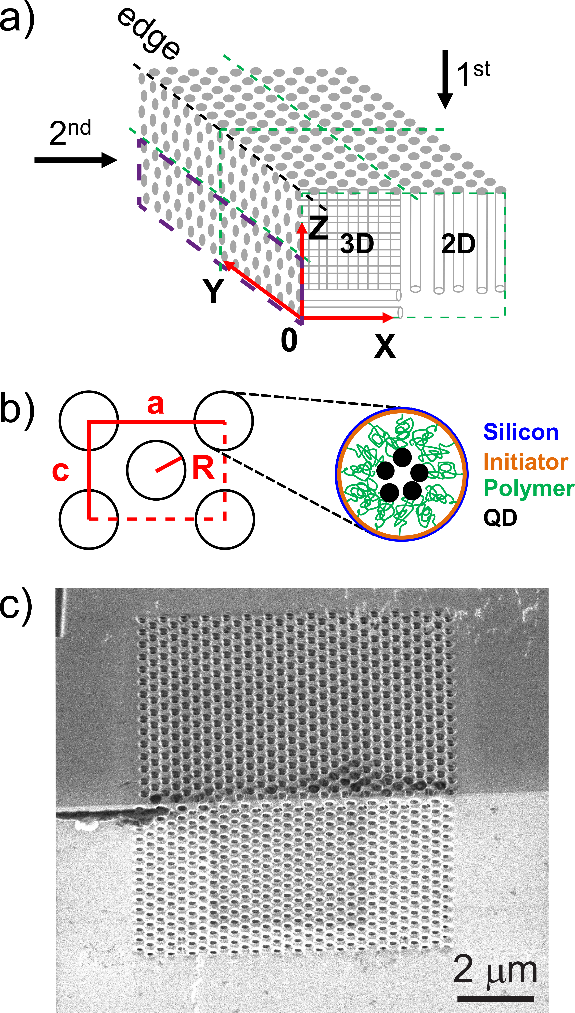 |
Figure 1 (a) Schematic of a 3D photonic crystal device that consists of two sets of pores etched in the Z-direction (1st set) and the X-direction (2nd set). In the region where the pores cross, the device has a 3D structure (otherwise 2D). Green dashed lines indicate the two surfaces into which nanopores are etched.
(b) View along the pores showing the lattice parameters (a,c) and pore radius R. Right: zoomed-in cross-section of one pore showing the surface-chemistry needed to infiltrate quantum dots: the orange layer are initiator molecules (“ATRP"), in green we indicate polymer chains that form so-called brushes, and the lead sulfide (PbS) quantum dots (black) are thus covalently attached on the silicon (blue).
(c) Scanning electron microscope (SEM) image of a real 3D photonic crystal as studied here, viewed from 45 degrees on the edge of a silicon wafer to show the XY (top) and the XZ surfaces (bottom). The scale bar indicates 2 micron. |
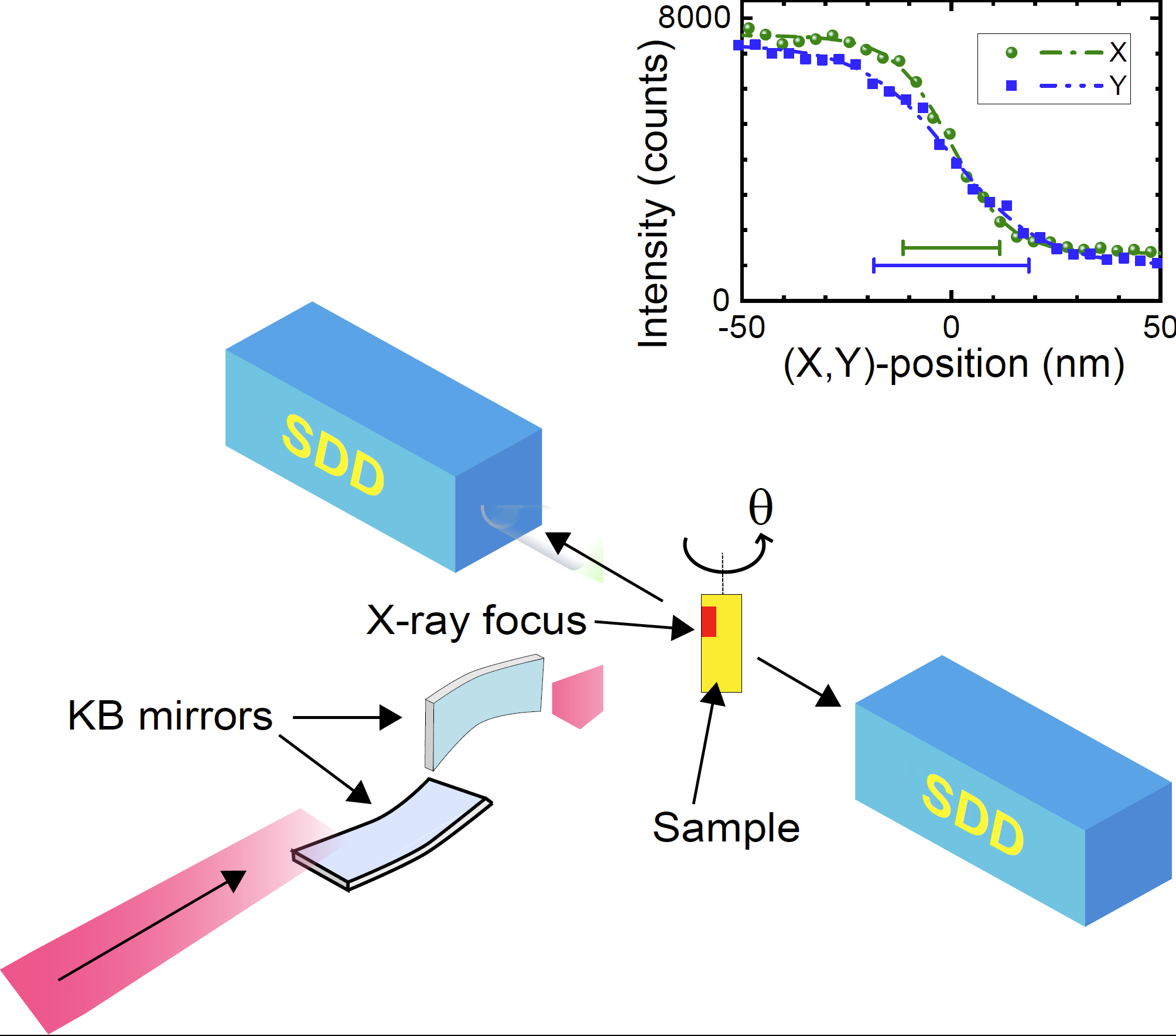 |
Figure 2: Schematic of the X-ray fluorescence imaging setup at ESRF beamline ID16A. The X-ray beam arrives from bottom left and is focused by Kirkpatrick-Baez (KB) optics on the sample. The fluorescent X-rays are detected by two silicon drift detectors (SDD) placed at 90 degrees with respect to the incident beam. The sample is rotated about angles q about the vertical axis. The inset presents measurements to characterize the cross-section of the excitation beam (intensity versus X- or Y -position) for a test sample. The resulting widths are DX = 23 nm and DY = 37 nm, which tells one how fine details can be seen. |
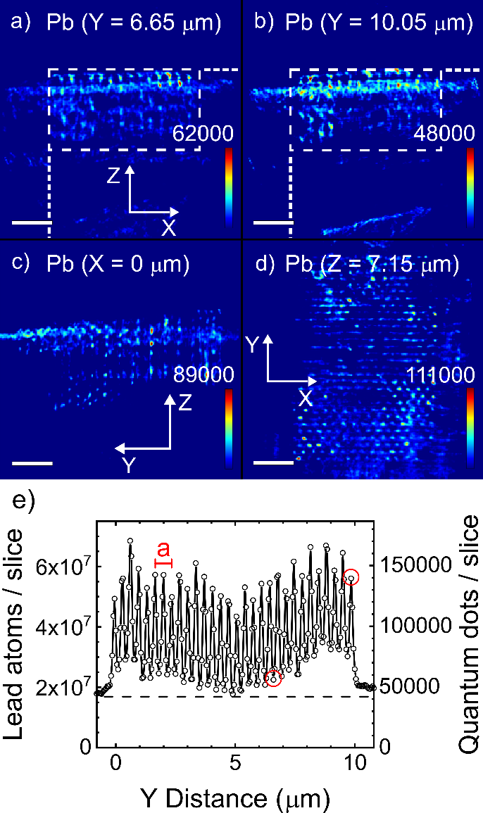 |
Figure 3: (a, b): XZ cross-sections of the reconstructed sample volume for the lead atoms at depths Y = 6.65 µm (a), Y = 10.05 µm (b). The scale bar represents 2 µm, the intensity bar the number of lead atoms per voxel and white dashed lines delineate the crystal's cross-section. The bright stripes show that the quantum dots are located all along the length of the pores: hooray! (c): YZ cross-section of the reconstructed sample volume for the lead atoms at depths X = 0 µm. (d): XY cross-section of the reconstructed sample volume for the Pb atoms at depths Z = 7.15 µm. e) Density of lead atoms per XZ-slice versus Y, the right ordinate shows the corresponding number of quantum dots (with 402 lead atoms per quantum dot). The lattice parameter a of our photonic crystal is indicated. The periodicity of the pores is clearly visible. The red circles show the Y-coordinates in (a) and (b). |
Reference
DOI: 10.1021/acsnano.1c06915
partners


European Synchrotron Radiation Facility - 71, avenue des Martyrs, CS 40220, 38043 Grenoble Cedex 9, France.