- Home
- Users & Science
- Scientific Documentation
- ESRF Highlights
- ESRF Highlights 2007
- Materials Science
- Void formation in Nb3Sn superconductors
Void formation in Nb3Sn superconductors
The formation of voids during the reaction heat treatment of Nb3Sn superconductors degrades their microstructural homogeneity and increases the strain sensitivity of the critical superconducting properties. The void formation mechanisms and possible remedies to limit void growth remain subjects of debate.
Previous studies of void growth in Nb3Sn strands have used destructive metallographic techniques. Since the void shape and distribution within Nb3Sn strands are strongly irregular, metallographic results about void formation are erratic and can be misleading. In contrast, by using synchrotron microtomography, a quantitative description of void volume, shape and distribution can be obtained. Owing to the short acquisition time of less than a minute per tomogram, tomography experiments during in situ heat treatments are routinely performed at beamline ID15A [1].
Here we report combined synchrotron microtomography and diffraction measurements during in situ heating cycles that have been performed at ID15A in order to reveal the void growth mechanisms in Nb3Sn strands of the internal tin (IT) design. Synchrotron microtomography was performed using a high intensity filtered white X-ray beam. For the diffraction measurements in transmission geometry, an 88.005 keV monochromatic X-ray beam with a bandwidth of 0.1 keV was used. Debye-Scherrer diffraction patterns were acquired with a MAR 345 image-plate detector. In situ heating was performed using a dedicated furnace built by ID15 that enables accurate sample temperature control during the tomographic and diffraction experiments.
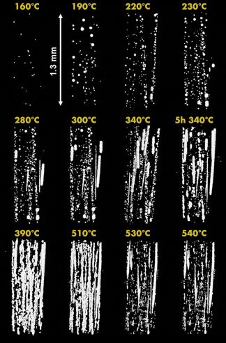
In Figure 23 the voids that are formed at different temperatures in the diffusion centres of the Nb3Sn strand are shown. The tomograms were acquired during an in situ heat treatment with a ramp rate of 60°C h-1, with three isothermal holding steps for 2 h at 200°C, 5 h at 340°C and 2 h at 540°C. Above 160°C the growth of globular voids is observed and the average shape factor (calculated from the ratio of void volume to void surface area) increases with increasing temperature. At 390°C the maximum total void volume is obtained (7.5 x 10⁻³ mm3, corresponding to 1.1% of the analysed strand volume). A strong reduction of total void volume from 5.7 x 10⁶ to 2.5 x 106 µm3 occurs in the temperature interval 510 to 530°C. During the isothermal 540°C heating, the number of the relatively small interfilament voids increases strongly.
 |
|
Fig. 23: Voids inside the IT Nb3Sn strand acquired at different temperatures during the in situ heat treatment. |
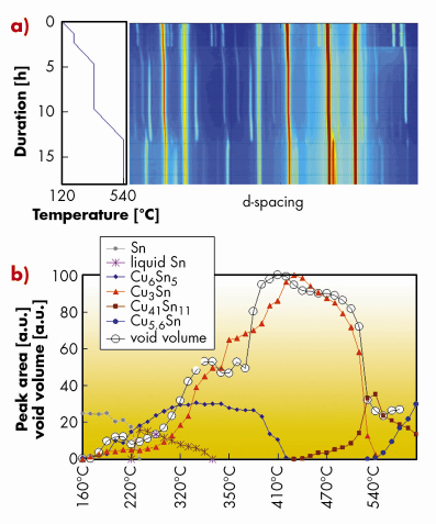
After the acquisition of each tomogram a diffraction pattern was acquired for phase analysis. The 110 diffraction patterns obtained during the heat treatment are summarised in Figure 24a.
During the first stage of the heat treatment up to 540°C five phase transformations are detected. At first pure Sn and Cu are transformed into Cu6Sn5 and Cu3Sn by solid state diffusion. At around 230°C the remaining Sn melts. Liquid Sn is present in the strand until 340°C and at 430°C nearly all Sn in the strand is transformed into Cu3Sn. The Cu3Sn reflections vanish in the temperature region 500 to 540°C and simultaneously a strong reduction in void volume occurs. Cu41Sn11 starts to form above 430°C. During the isothermal 540°C heat treatment, Cu5.6Sn peaks grow until the formation of Nb3Sn starts at about 580°C (Nb3Sn growth results are not shown in Figure 24).
 |
|
Fig. 24: a) Variation of the diffraction patterns of the Nb3Sn strand during the heat treatment cycle between 120°C and 540°C. b) Diffraction peak areas of all Sn-containing phases, apart from |
Combining the microtomography and the diffraction results, three different void-growth mechanisms in IT Nb3Sn superconductors can be deduced. The growth of the globular voids up to a temperature of about 200°C is driven by a gain in free energy through a reduction of the total void surface area when smaller voids agglomerate to larger globular voids. The main void volume increase is caused by density changes during the formation of Cu3Sn (the Cu3Sn density exceeds the density of stoichiometric Sn and Cu by 4%). Therefore, the maximum void volume is obtained when Sn is almost entirely transformed into Cu3Sn. The void growth caused by density changes is partly reversible when Cu-Sn intermetallics are transformed into the lower density ![]() -bronze. The relatively small interfilament voids that grow at the Cu-Sn intermetallic/a-bronze interface during the isothermal 540°C heat treatment and at higher temperatures are Kirkendall voids.
-bronze. The relatively small interfilament voids that grow at the Cu-Sn intermetallic/a-bronze interface during the isothermal 540°C heat treatment and at higher temperatures are Kirkendall voids.
Principal publication and authors
C. Scheuerlein (a), M. Di Michiel (b), A. Haibel (c), Appl. Phys. Lett. 90, 132510 (2007).
(a) European Organization for Nuclear Research (CERN), Geneva (Switzerland)
(b) ESRF
(c) Hahn-Meitner Institut Berlin (HMI) (Germany)
References
[1] M. Di Michiel, J.M. Merino, D. Fernandez-Carreiras, T. Buslaps, V. Honkimäki, P. Falus, T. Martins, O. Svensson, Rev. Sci. Instrum.76, 043702 (2005).


