- Home
- Users & Science
- Scientific Documentation
- ESRF Highlights
- ESRF Highlights 2011
- Structure of materials
- Does liquid-ordering play a role in determining the crystallographic structure of nanowires?
Does liquid-ordering play a role in determining the crystallographic structure of nanowires?
Semiconducting nanowires offer the possibility of nearly unlimited complex bottom-up design, which allows new device concepts that may find use in applications like sensors, solar energy conversion or light-emitting diodes. Essential parameters that determine the electronic and optical properties of a nanowire are its crystal structure and the density of defects.
Nanowires can be grown from nano-sized metal droplets by the vapour-liquid-solid (VLS) growth mechanism. As the name suggests, three phases are involved in this type of nanowire growth. Precursor molecules from the gas phase are decomposed and form an alloy with the metal particle. Nucleation occurs at the solid-liquid interface and the crystalline nanowire grows layer by layer. The crystal structure of nanowires grown by the VLS mechanism is often different from corresponding bulk crystals. For instance, intrinsic InP nanowires crystallise in the wurtzite structure, while bulk, Czochralski-grown InP crystals have the zinc-blende structure. It has been argued that the shape of the metal particle, and more specifically the contact angle of the droplet with the nanowire side facets, determines the nanowire crystal structure [1], but alternatively the chemical composition and the precise atomic positions at the solid-liquid interface could determine the nanowire crystal structure [2]. We used surface X-ray diffraction at beamline ID03 to solve the atomic structure at the liquid-solid interface of an AuIn alloy in contact with a (111) InP bulk crystal surface at elevated temperatures, simulating the solid-liquid interface during InP nanowire growth from an initial Au particle.
Two major problems are encountered when studying the solid-liquid interface of genuine nanowires in situ. First, the actual area covered by nanowires is quite small, and second, growth conditions are required with highly-toxic precursor gasses. We therefore used a thin alloy film in contact with an InP (111) substrate as a model system. The InP substrate is covered by a 100 nm metal layer, with the eutectic composition of the AuIn alloy. To minimise the decomposition of the InP substrate by phosphorus desorption during heating, a 100 nm SiO2 layer was deposited on top as a protective layer. The samples are heated to 773K to liquefy the AuIn alloy, similar to the annealing steps prior to nanowire growth. Then, the samples were cooled down to 693K, a typical growth temperature for InP nanowire growth.
 |
|
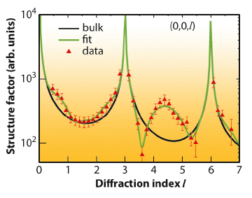
Fig. 50: The experimental structure factors (triangles) together with the optimum fit (green curve) that shows the exceptional high degree of liquid ordering in the Au-In eutectic at the measurement temperature of 693 K. The black curve shows the expected shape without liquid ordering. Additional data (not shown) yield the lateral location of the first-layer liquid atoms. |
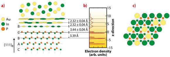
By measuring specular and non-specular rods, both the in-plane and out-of-plane structures of the solid-liquid interface are determined. The experimental data (Figure 50) are fitted to a model (Figure 51a) that describes the entire solid-liquid interface. We find that several of the liquid layers show a surprisingly high degree of order. Moreover, the first layer has an increased In composition and the atoms are positioned in the middle of the InP hexagons of the crystal surface (Figure 51c). This can have important consequences for the structure (stacking) of the next InP layer. When nucleating the next crystalline bilayer, In will always be positioned on top of the P atoms of the previous bilayer. Only the P atoms in the new layer will determine the stacking. There are two possibilities, either continuing the zinc-blende structure or forming a stacking fault, corresponding to the start of the wurzite structure. Because we find that the hollow sites are preferentially occupied by Au/In alloy atoms, the P atoms will be sterically-hindered for entry into the zinc-blende positions and therefore crystallise preferentially in the wurtzite structure.
 |
|
Fig. 51: a) A side view of the solid-liquid interface structure of the InP crystal in contact the Au-In eutectic. The first quasi-liquid layer has a B stacking and is enriched in In. b) The z-projected electron density distribution as derived from the data in Figure 50. c) Top-view of the InP surface (small circles) indicating that the first liquid layer (large circles) occupies the centre of the hexagonal InP rings. |
Principal publication and authors
R. Algra (a,b), V. Vonk (a), D. Wermeille (c), W. Szweryn (a), M. Verheijen (b), W. van Enckevort (a), A. Bode (a), W. Noorduin (a), E. Tancini (c), A. de Jong (a), E. Bakkers (b) and E. Vlieg (a), Nano Lett. 11, 44–48 (2011).
(a) Radboud University Nijmegen, Institute for Molecules and Materials (The Netherlands)
(b) Philips Research Laboratories Eindhoven (The Netherlands)
(c) ESRF
References
[1] F. Glas, J. Harmand and G. Patriarche, Phys. Rev. Lett. 99, 146101 (2007).
[2] R. Algra, M. Verheijen, M. Borgström, L. Feiner, G. Immink, W. van Enckevort, E. Vlieg and E. Bakkers, Nature 456, 369-372 (2008).


