- Home
- Users & Science
- Scientific Documentation
- ESRF Highlights
- ESRF Highlights 2011
- Structure of materials
- Shedding light on the heart of a transistor
Shedding light on the heart of a transistor
X-ray diffraction is a powerful tool to determine the structural properties of all manner of materials. The absence of specific requirements for sample preparation makes it one of the most appealing methods to check quickly the sample quality and to gain crucial information on new materials. A limiting factor for nanoscale structures is the lack of spatial resolution, as the diameters of X-ray beams are usually in the range from millimetres down to few tens of micrometres. We used the latest advances in technology for hard X-ray focusing and precise sample positioning available at beamline ID01 to explore the centre of a fully processed transistor device, an area size well below one micrometre.
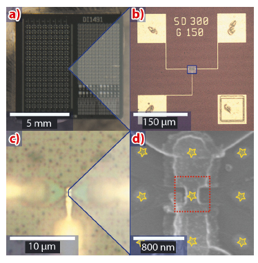
The investigated device was a ‘dot-FET’ [1], an n-type field-effect transistor with a strained silicon channel as its main active element and a SiGe island (or dot) as stressor. Strain engineering is a versatile tool to enhance the properties of a transistor such as carrier mobility, in this case electrons, and thereby the switching speed. Si and Ge have the same crystal structure with a lattice mismatch of 4.2%, thus a Ge layer can be used to stretch the lattice of Si grown on top. In the dot-FET, a self-organised 3D SiGe island with 250 nm diameter and 50 nm height is used to apply tensile strain to the Si channel. Its enhanced relaxation compared to 2D layers enables higher strain values while avoiding defects. Such islands are grown on pre-patterned Si (001) substrates as the transistor needs to be aligned with high precision around a single island (see Figure 35d). In the completed device this small active area is buried underneath the gate stack, metal contacts and insulation layers, which makes it hard to assess its structural properties while preserving its functionality.
 |
|
Fig. 35: Photograph a) and optical micrographs (b, c) of the sample at different scales. d) shows a SEM image of a transistor sample after gate formation, before source and drain contacts are in place. The gate finger is precisely aligned to the array of SiGe islands (asterisks). The red square marks the area probed by the X-ray beam. |
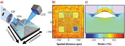
XRD with a focused beam of 400 nm diameter FWHM offers the possibility to probe exclusively this small area. The setup for focusing hard X-ray beams at ID01 is shown in Figure 36a. Via scanning X-ray diffraction (SXD, see Figure 36b) [2], we were able to identify the specific island at the transistor core and record reciprocal (004) and (224) space maps to derive parameters such as the average Ge content of the island or the thickness of the Si capping layer. Here, the Si channel was reduced from 30 nm in the as-grown sample to about 24 nm in the completed device due to processing steps including gate stack deposition, etching, implanting and annealing. Combining XRD measurements with finite element simulations, we found tensile strain values of 1% in the Si channel, which are locally reduced due to the influence of the gate stack (see Figure 36c).
Such investigations are highly valuable for the development of process flows, as samples from different processing steps can be compared without destructive preparation. Furthermore, the investigation of devices during operation becomes feasible, which is important e.g. for ageing and reliability studies.
Principal publication and authors
N. Hrauda (a), J.J. Zhang (a,b), E. Wintersberger (a,c), T. Etzelstorfer (a), B. Mandl (a), J. Stangl (a), D. Carbone (d), V. Holý (e), V. Jovanovic (f,g), C. Biasotto (f,h), L.K. Nanver (f), J. Moers (i), D. Grützmacher (i) and G. Bauer (a), Nano Letters 11, 2875–2880 (2011).
(a) Institute of Semiconductor and Solid State Physics, JKU Linz (Austria)
(b) IFW Dresden (Germany)
(c) HASYLAB at DESY, Hamburg (Germany)
(d) ESRF
(e) Faculty of Mathematics and Physics, Charles University Prague (Czech Republic)
(f) DIMES, TU Delft (The Netherlands)
(g) FER, University of Zagreb (Croatia)
(h) CCS, State University of Campinas, São Paulo (Brazil)
(i) Halbleiter-Nanoelektronik (IBN-1), Forschungszentrum Jülich GmbH (Germany)
References
[1] V. Jovanovi’c, C. Biasotto, L.K. Nanver, J. Moers, D. Grützmacher, J. Gerharz, G. Mussler, J. van der Cingel, J.J. Zhang, G. Bauer, O.G. Schmidt and L. Miglio, IEEE Electron Device Letters 31, 1083–1085 (2010).
[2] C. Mocuta, J. Stangl, K. Mundboth, T.H. Metzger, G. Bauer, I.A. Vartanyants, M. Schmidbauer and T. Boeck, Phys. Rev. B 77, 245425 (2008).


