- Home
- Users & Science
- Scientific Documentation
- ESRF Highlights
- ESRF Highlights 2011
- Structure of materials
- Acids attack: tracing rapid metal etching on the atomic scale
Acids attack: tracing rapid metal etching on the atomic scale
Chemical etching and coating of metals have numerous important industrial applications, ranging from metal mining and refinement to high-tech processes such as the metallisation of ultra large scale integrated microchips. Because of these important applications, the structural changes in materials during etching and coating are intensively studied worldwide. Such studies at present largely fall into two categories. Firstly, studies of the structure of real specimens from the actual technological process analysed ex situ, i.e., after the etching or deposition reaction. This is commonly the case in applied research, however, direct insight into the morphological evolution is difficult to obtain and artefacts (e.g. changes in the sample structure during sample emersion and transfer) cannot be rigorously excluded. The second category, particularly in the last two decades, includes fundamental studies of growth and etching processes at solid-liquid interfaces that have been performed by high-resolution in situ methods. In particular, scanning probe microscopy and synchrotron-based X-ray techniques have contributed enormously to the in-depth understanding of these complex interface processes by revealing in detail the mechanisms of nucleation and growth on the atomic scale. However, all these techniques have been limited to studies at deposition or dissolution rates that are orders of magnitude lower than those employed in industrial processes. Hence, similar to heterogeneous catalysis, a substantial gap exists between atomic-resolution in situ studies and the corresponding industrial applications.
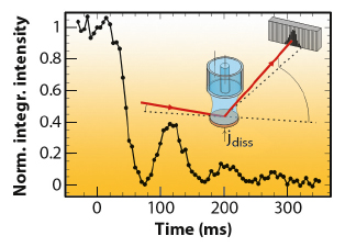
In recent years, in situ surface X-ray scattering (SXS) studies of electrochemical metal deposition and dissolution in acidic solutions have been pioneered at beamline ID32. The use of electrochemical cells with transmission geometry (see inset in Figure 42) has allowed the study of reactions with unrestricted mass transport. In the initial in situ experiments with such cells, the homoepitaxial electrochemical metal deposition and dissolution in Cl-containing electrolytes were studied on the atomic scale at moderate rates of a few monolayers per minute, revealing a complex growth behaviour that depends on the applied potential and the interface structure [1,2].
 |
|
Fig. 42: Growth oscillations indicating layer-by-layer growth for Au(001) dissolution in 0.1 M HCl + 0.5 mM HAuCl4, after a potential step from 0.60 to 1.07 VAg/AgCl, where anodic etching commences. The inset illustrates the diffraction geometry. |
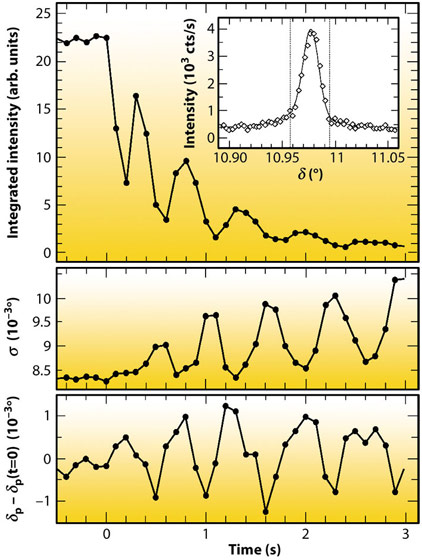
Recently, we reported significant advances in this method that allowed studies to be performed at rates close to those employed in technological processes. Key to this improvement was the implementation of a state-of-the-art solid state 1D pixel detector (Dectris Mythen 1K) on the ID32 six-circle diffractometer. This permits single-shot studies of surface structural changes with a time resolution of few milliseconds, which is essential for investigating irreversible processes, such as crystal growth and etching. We studied the anodic electrochemical dissolution of Au(001) in HCl solution by grazing incidence X-ray scattering (EPh= 22.5 keV). The time-dependent intensity of the crystal truncation rod was recorded close to the anti-Bragg position by the 1D detector (Figure 42). After applying a potential step into the regime of anodic gold etching, characteristic growth oscillations are observed that indicate a layer-by-layer dissolution mechanism up to electrochemical currents of 10 mA cm-2, corresponding to dissolution rates as high as 20 ML/s. These rates are already comparable to those employed in microchip metallisation. Furthermore, each cycle of the pixel detector contained information on the peak position and width (Figure 43), providing insight into strain and lateral correlations at the metal surface. Both position and width exhibit clear oscillations, which are in agreement with a layer-by-layer dissolution mechanism, where the surface alternates periodically between a smooth and a vacancy island covered state.
 |
|
Fig. 43: Oscillatory behaviour of intensity (top), peak width σ (middle), and peak position δP (bottom) of the (1,1,0.1) peak during Au(001) dissolution at 0.99 VAg/AgCl, indicating alternating surface strain and lateral correlations during layer-by-layer etching. |
More recently, we applied this method to the important case of galvanic copper deposition on Cu(100) in chloride-containing acidic electrolytes. Contrary to previous STM studies at low growth rates, potential-dependent transitions to layer-by-layer and even 3D mode were detected, illustrating the need to extend atomic-scale studies into the range of more realistic deposition rates.
In summary, the highly brilliant hard X-ray beam of the ESRF together with fast photon-counting area detectors provide unique opportunities for studying structural changes at deeply buried solid-liquid interfaces under realistic conditions. This approach will also be of great use for in-depth investigations of other (electro-) chemical processes and eventually may help to close the gap between fundamental studies of model systems and applied studies of fast technological or natural reactions.
Principal publication and authors
F. Golks (a,b,c), K. Krug (a,d), Y. Gründer (a,e), J. Zegenhagen (b), J. Stettner (a) and
O.M. Magnussen (a), J. Am. Chem. Soc. 133, 3772-3775 (2011).
(a) Institut für Experimentelle und Angewandte Physik, Universität Kiel (Germany)
(b) ESRF
(c) Robert Bosch GmbH, Suttgart (Germany)
(d) Present address: Department of Chemical Engineering, National Cheng University (Taiwan)
(e) Present address: The School of Chemistry, University of Manchester (UK)
References
[1] K. Krug, J. Stettner and O.M. Magnussen, Phys. Rev. Lett. 96, 246101 (2006).
[2] K. Krug, D. Kaminski, F. Golks, J. Stettner and O.M. Magnussen, J. Phys. Chem. C 114, 18634 (2010).


