- Home
- Users & Science
- Scientific Documentation
- ESRF Highlights
- ESRF Highlights 2015
- Enabling technologies
- Diffraction topography as an industrial tool for the characterisation of the crystalline quality of diamond
Diffraction topography as an industrial tool for the characterisation of the crystalline quality of diamond
Beamline BM05 provides powerful tools for the characterisation of the crystalline quality of synthetic single crystal diamonds. White beam “topography” imaging is a fast and straightforward technique that is capable of identifying all the extended crystal defects. Using this method, we detected differences in the crystal quality such as dislocation densities and growth sectors between commercially available diamond plates from various suppliers. A quantitative extension of this diffraction imaging technique is rocking curve imaging using a monochromatic beam. This allows determination of the lattice parameter variations and the local lattice tilts. This can be related to the presence of specific defects and also the lattice deformation induced by impurity incorporation, for example due to boron doping, which is differentiated according to the local growth conditions.
Synchrotron techniques have been used for both academic and industrial studies to characterise silicon and diamond. X-ray Bragg diffraction imaging (“X-ray topography”) is a well-known technique for characterising crystalline quality. The various Bragg diffraction imaging techniques (white beam topography, rocking curve imaging and others) have been implemented at beamline BM05, where they are used for research and as standard techniques to characterise the quality of crystals for industrial applications. This method is sensitive to defects such as dislocations, stacking faults, surface imperfections, even weak simple impurity concentration gradients and inclusions via the distortion they induce in the crystal lattice and allows their spatial structure to be investigated with a resolution down to the micrometre scale.
Interest in single crystal diamond for electronic applications is increasing because of its many attractive physical and electronic properties, in particular its wide band gap, high mobility of both charge carriers, high electric field breakdown strength, low X-ray absorption coefficient, low thermal expansion and extremely high thermal conductivity. Our interests are the application of diamond in the related fields of electronics and detectors, and diffractive and refractive optics, where many of the previously mentioned properties are particularly relevant. Boron and phosphorus doped diamond devices have already been shown to allow the fabrication of excellent high voltage diodes and FET switches. These are expected to efficiently commute high power at high frequency. The Horizon2020 European project Green Diamond [1] is a four year 4.5 M€ project that aims to develop all-diamond high power electronic devices, with the goal of substantially reducing the huge energy losses associated with electrical power transmission and transport. The ESRF is one of the 14 institutes participating in Green Diamond, playing a vital role in characterising the diamond material: hundreds of the [100] orientation plates needed by the project have already been measured at BM05. High quality diamond plates are also needed at modern synchrotrons for X-ray optical applications. Another potential application relies on the creation of a diamond superlattice by the periodic concentration variation of boron-doping during synthesis. A controlled periodic variation of the lattice parameter can be achieved while maintaining coherent lattice quality. Using high energy charged particle beams, diamond crystal undulators fabricated in this manner could theoretically generate powerful monochromatic radiation reaching up to g-ray energies.
 |
|
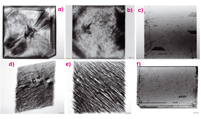
Fig. 141: White beam topography of different single diamond plates characterised at BM05: (a) HPHT, (b) CVD E6, (c) HPHT NDT, (d) CVD EDP, (e) Diam2tech, (f) IIa. |
Such applications all require defect free (surface and bulk) diamond plates with high quality polished surfaces of well controlled (~ 0.1°) miscuts. The commercial availability of single crystal diamond substrates from various suppliers covers a large variety of crystalline qualities and prices. Examples of topography measurements made at BM05 are shown in Figure 141: The high quality type-IIa diamond samples (Figure 141c and f) show areas that are almost dislocation free in the large 100 growth sector, with only a few stacking-faults and surface scratches visible.
 |
|
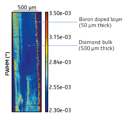
Fig. 142: Diamond 400 reflection FWHM maps obtained using section topography rocking curve imaging. The scale is in degrees and shows the variation in crystalline quality in a virtual cross-section through a 500 μm thick diamond plate overgrown with a 50 μm thick Boron doped diamond layer. The face with the Boron doped layer is on the right. |
The other ‘low grade’ commercial diamond plates shown present dislocations with densities of 103 to 104cm–3. Figure 142 shows a quantitative measurement of the crystalline quality (assessed via the rocking curve width) of a boron doped layer grown on a diamond plate. The image suggests a correlation between the boron doped layer with distortion of the diamond surface: the rocking curve (FWHM > 3.5° x 10–3) is much higher at the boron doped border than at the sample centre bulk region (FWHM 2.4° x 10–3).
Particular attention must be paid not only to the quality of overgrown doped diamond layers, but also to the diamond substrate itself, including all the defects that exist in the bulk such as dislocations, stacking faults, growth sectors, and (sub) surface damage from polishing processes. In the case of electronic devices, all of these defects contribute to the final performance.
Authors
T.N. Tran Caliste (a), J. Hartwig (a), J. Morse (a), E. Ziegler (a), R. Barret (a) and S. Connell (b).
(a) ESRF
(b) University of Johannesburg (South Africa)
References
[1] GreenDiamond: www.greendiamond-project.eu


