- Home
- Users & Science
- Scientific Documentation
- ESRF Highlights
- ESRF Highlights 2015
- X-ray nanoprobe
- Individual GaAs nanowires: a correlation of electrical and structural properties
Individual GaAs nanowires: a correlation of electrical and structural properties
The electrical response of individual as-grown GaAs nanowires on the original silicon substrate has been correlated with their structural quality. The electrical characteristics of single nanowires were measured in a focused ion beam chamber and their polytype composition determined using X-ray nano-diffraction.
Semiconductor nanowires in as-grown geometry on their substrate are promising building blocks for novel electronic, photonic and optoelectronic devices. The electronic band structure and functionality of those devices can be strongly influenced by the crystalline purity of the constituent materials and the presence of different polytypes, such as zinc-blende, twinned zinc-blende and wurtzite. The nanowires under investigation were grown on a Si substrate along the (111) direction with diameter of 100 nm and height of about 1 µm by means of self-assisted molecular beam epitaxy (MBE). Before growth, periodic openings were fabricated through the SiO2 thermal oxide layer by electron beam lithography with a pitch distance of 2 µm. This allowed the nanowires to be grown only at pre-defined positions across the substrate surface.
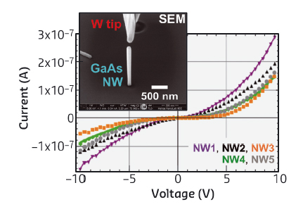
Individual free-standing GaAs nanowires were electrically investigated in a dual-focused ion beam (FIB) system. Nanometre-sized tungsten needles with a mean radius of 30 nm were used to contact the top of a selected nanowire. A second contact was made onto the conducting substrate. Subsequently, voltage-current (V-I) characteristics (Figure 8) with a voltage varying between -10 V and +10 V were measured using a semiconductor analyser. The inset in Figure 8 shows the contacting needle close to the top of a single nanowire. Two different electrical regimes were identified in the electrical characteristics: a back-to-back Schottky diode regime, complying with the thermoionic emission theory, and a space charge limited current regime. Effective mobility and resistance values were extracted for different nanowires, having 10 cm2/Vs and 102 MΩ respective orders of magnitude. To check the reproducibility of the measurements, each nanowire was contacted several times by approaching the W tip to the top and applying different pressures. The current-voltage curves collected were compared to quantify the influence of the contacting procedure, and this constitutes the uncertainty in our measurements.
 |
|
Fig. 8: Voltage−current characteristics of several nanowires (NWs). Inset: Scanning electron microscope (SEM) image of a tungsten contacting needle close to the top of an individual nanowire inside the FIB chamber. |
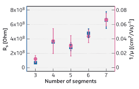
To determine the origin of the differences detected, the structure of the same individual nanowires was investigated using nanofocused X-ray Bragg diffraction [1,2] at beamline ID01. To identify the very same nanowires previously characterised in the FIB chamber, Pt-markers (easily detectable with an optical microscope) were deposited simultaneously in the FIB chamber by a gas injector system close to the position of interest. The X-ray beam used had a photon energy of 7.8 keV, and was focused with a Fresnel Zone Plate (FZP) down to a focal size of 400 x 700 nm2 providing the spatial resolution required to achieve single nanowire inspection. During the X-ray exposure, a constant nitrogen flux was blown over the sample to protect the nanowires from possible radiation-induced oxidation. To identify the nanowire to be measured, X-ray nano-diffraction maps of large areas on the sample surface were collected under Bragg conditions using the K-map method [3]. For accurate structural characterisation, intensity maps were collected as a function of the three components of the wave vector transfer, i.e. reciprocal space maps, at the structurally sensitive [4] asymmetric (331), (422) and (1015) reflections. The structural investigation revealed the presence of several zinc-blende and twinned zinc-blende segments, stacked above each other and most likely separated by multiple stacking faults. A correlation was found between the number of these units and the extracted electrical parameters (Figure 9). A monotonic increase of the resistive behaviour with the number of segments, and therefore phase boundaries, was observed. The origin of this specific structural configuration may be related to the pressure exerted onto the nanowire during the electrical characterisation. The role played by the contacting procedure acquires therefore great importance. A small plastic deformation may lead to the simultaneous activation of several secant {111} glide planes, and change the nature of the phase boundaries by enhancing the number of stacking faults.
 |
|
Fig. 9: Total extracted resistance (Rs) and inverse effective mobility (1/µ) as functions of the number of segments (interfaces) within the nanowires. |
In conclusion, a method for correlating the differences in the V−I characteristics with the number of intrinsic interfaces within the same individual nanowire was demonstrated. It is suitable for the collection of valuable data for the improvement of growth and contacting techniques, towards tuneable electrical properties.
Principal publication and authors
Correlation of Electrical and Structural Properties of Single As-Grown GaAs Nanowires on Si (111) Substrates, G. Bussone (a,b), H. Schäfer-Eberwein (c), E. Dimakis (d,e), A. Biermanns (b), D. Carbone (a), A. Tahraoui (d), L. Geelhaar (d), P. Haring Bolívar (c), T.U. Schülli (a) and U. Pietsch (b), Nano Lett. 15, 981-989 (2015); doi: 10.1021/nl5037879.
(a) ESRF
(b) Festkörperphysik, Universität Siegen (Germany)
(c) Hochfrequenztechnik and Quantenelektronik, Universität Siegen (Germany)
(d) Paul-Drude-Institut für Festkörperelektronik, Berlin (Germany)
(e) Helmholtz-Zentrum Dresden-Rossendorf, Institute of Ion Beam Physics and Materials Research, Dresden (Germany)
References
[1] A. Biermanns et al., J. Synchrotron Rad. 16, 796-802 (2009).
[2] G. Bussone et al., J. Appl. Crystallogr. 46, 887-892 (2013).
[3] G.A. Chahine et al., J. Appl. Crystallogr. 47, 762-769 (2014).
[4] A. Biermanns et al., J. Appl. Crystallogr. 45, 239-244 (2012).


