- Home
- News
- Spotlight on Science
- Oxygen doping level...
Oxygen doping level tuning in the Bi-2212 superconductor by X-ray nano-beam irradiation
26-06-2014
Hard X-rays could be used as a novel direct-writing, photoresist-free lithographic process with potential nanometric resolution and 3D capability, thus overcoming the current limitations in the fabrication of miniaturised devices. A team of researchers from Turin used the ESRF’s X-ray nanoprobe to explore the controlled use of a 17 keV X-ray synchrotron nanobeam to progressively change the oxygen doping level in Bi-2212 superconducting oxide microcrystals. Their research demonstrates that irradiating this material with high X-ray doses results in an elongation of the c-axis and in an increase of the critical temperature.
Share
In the past few decades, the goal of achieving higher speed and lower power consumption has driven the semiconductor industry to design and produce smaller and smaller integrated circuits. This trend has stimulated deep innovation in lithographic techniques based on the use of short wavelength radiation. Nevertheless, hard X-rays based lithography with λ ≈ 0.1 nm has been hampered by problems related to the fabrication of suitable masks with both high enough contrast in their absorbing power and small enough features. Another appealing possibility is represented by direct-writing techniques allowing modification of the substrate properties without using a photoresist. Among these techniques, focused-electron-beam- and the focused-ion-beam-induced deposition and etching, along with scanning-probe lithography, are the most commonly used, and all enable nanometric spatial resolution [1, 2]. Concerning X-ray direct-writing lithography, a few examples have been recently reported, but limited to organic or organometallic materials. Nevertheless, some experiments have shown that synchrotron radiation can modify the properties of inorganic materials directly by means of photon-induced displacement of light atoms in their crystal structure [3].
We have explored the application of X-ray direct-writing lithography to the superconductor Bi2Sr2CaCu2O8+δ (Bi-2212), which features typical Tc values of 80-90 K. As Bi-2212 crystals at temperatures below Tc emit and absorb THz radiation [4], an obvious application of direct-writing lithography could be the production of Bi-2212 based devices. Direct-writing X-ray lithography is particularly interesting because of the expected increase in availability of hard X-ray sources with very high brilliance and power, including new and upgraded synchrotron and XFEL sources.
 |
|
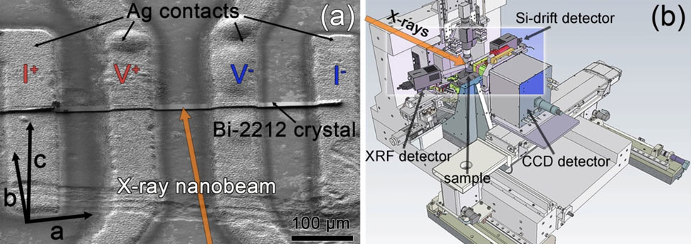
Figure 1. a) SEM micrograph of a typical chip used for experiments on the Bi-2212 microcrystals. Current and voltage electrodes used for the four-probe technique are labeled as I+, I-, V+ and V-, respectively. The orange arrow indicates the nanobeam position used during the irradiation sessions. b) Scheme of the experimental setup used at the ID22NI beamline. |
Our investigation focused on the effect of localised hard X-ray irradiation on Bi-2212 microcrystals (see Figure 1a) using the 117 × 116 nm2 nanoprobe available at the ID22NI beamline (now installed at the upgraded beamline ID16B), see Figure 1b. The structural modification induced by the X-ray nanobeam was monitored using nano-XRD, while the corresponding change in the electrical properties was measured via a standard four-probe method after each irradiation session. We found that irradiating this material with 17 keV X-rays with doses in the order of 1012 Gy results in an elongation of the c-axis and in an increase of both the critical temperature and the normal state resistivity (see Figure 2). This evidence points to modification in the oxygen doping level of the material, changing from an over-doped state towards a progressively more under-doped one.
 |
|
Figure 2. a) Four-probe ab-plane resistivity versus temperature curves for the Bi-2212 micro-crystal in as-grown conditions and after increasingly higher X-ray doses. The insets report a magnification of the transition region and the Tc versus resistivity dependence at room temperature for each of the four experimental conditions. b) Dependence of the c-axis length and of Tcon the X-ray dose. |
Moreover, modeling the various experimental conditions by means of the finite element method (FEM, see Figure 3) allowed us to exclude heating induced by the X-ray nanobeam as a possible cause for the change in the doping level. Conversely, an important role is suggested for the photoelectrons as a possible source for knock-on effects on the oxygen atoms in the BiO layers, due to their low displacement threshold energy, which has already been predicted for the oxygen atoms in the CuO chains of YBCO [5].
 |
|
Figure 3. Temperature field induced by the synchrotron nanobeam on the Bi-2212 sample according to FEM simulations. |
These results pave the way to a novel direct-writing X-ray nanolithography approach, with an ultimate resolution in the range of the photoelectron inelastic mean free path (~ 10 nm), possibly exceeding the present limits of focused-electron-beam and focused-ion-beam lithography in terms of contamination, mechanical stability and 3D fabrication capability.
Principal publication and authors
A. Pagliero (a), L. Mino (b), E. Borfecchia (b), M. Truccato (a), A. Agostino (b), L. Pascale (b), E. Enrico (c), N. De Leo (c), C. Lamberti (b), Gema Martínez-Criado (d), Doping change in the Bi-2212 superconductor directly induced by a hard X ray nanobeam, Nano Lett. 14, 1583 (2014).
(a) Department of Physics, NIS Centre of Excellence, University of Turin, Torino (Italy)
(b) Department of Chemistry, NIS Centre of Excellence, University of Turin, Torino (Italy)
(c) INRIM, National Institute of Metrological Research, Torino (Italy)
(d) ESRF
References
[1] S.J. Randolph et al., Crit. Rev. Solid State Mat. Sci. 31, 55 (2006).
[2] A.A. Tseng et al., J. Vac. Sci. Technol. 23, 877 (2005).
[3] N. Poccia et al., Nat. Mater. 10, 733 (2011).
[4] L. Ozyuzer et al., Science 318, 1291 (2007).
[5] I. Piñera et al., Phys. Stat. Sol. A 204, 2279 (2007).
Top image: SEM micrograph of a typical chip used for experiments on the Bi-2212 microcrystals.
partners


European Synchrotron Radiation Facility - 71, avenue des Martyrs, CS 40220, 38043 Grenoble Cedex 9, France.