- Home
- News
- General News
- Dark-field X-ray...
Dark-field X-ray microscopy provides surprising insight on ferroelectrics
25-06-2018
Thanks to the unique capabilities of in-situ dark-field X-ray microscopy, scientists have now been able to see the complex structures hidden deep inside ferroelectric materials. The results, published today in Nature Materials, contradict previous studies in which only the surface was studied. This revolutionary new technique will be the main feature of a new beamline for the new EBS machine currently being built at the ESRF.
Share
“Until now we could only see the surface of the material; dark-field x-ray microscopy is like creating a window to its interior", explains Hugh Simons, assistant professor at the Technical University of Denmark and corresponding author of the study. “It provides incredible contrast for even the subtlest structures inside these materials, giving us a much clearer picture of how they work”, he adds.
Simons, together with the team of ID06 - the beamline where the technique is being developed - studied the ferroelectric material BaTiO3, which is used every day in cars, computers and mobile phones. By imaging their internal structure at the same time as they applied an electric field on it, they could see how these internal structures behave and change dynamically.
 |
 |
|
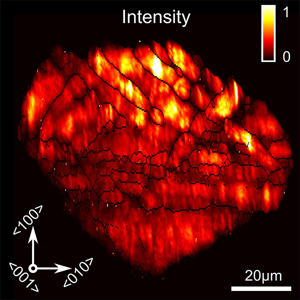
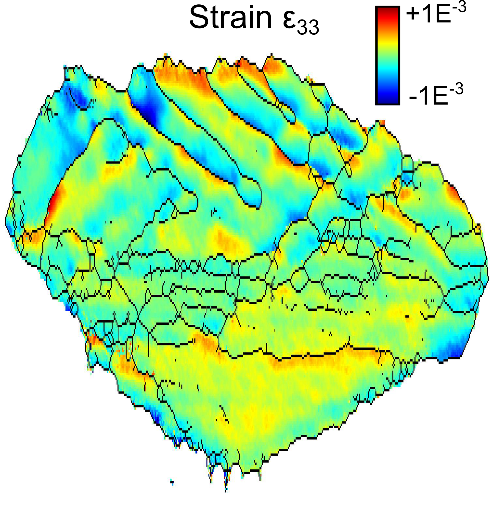
Crosssectional dark-field x-ray microscopy maps of the embedded BaTiO3 grain. Individual domains are visible in the integrated intensity image (left), while the reconstructed strain (right) map reveals the structural relationship between domain clusters. Credit: H. Simons. |
|
Ferroelectric materials work thanks to the symmetry of their crystalline structure. So, when defects in the material create strain fields that break this symmetry, it can have a dramatic effect on the properties. Understanding the way these defects strain and distort the material then opens the way to making new materials with much better properties than ever before.
During the experiment, the team measured the distortions around two particularly prevalent types of defect in many ferroelectrics: domain walls and grain boundaries. Previous studies suffered from the technical limitation that they could only work with surfaces or very thin films. They could therefore not access deeply buried grains that are strained in all directions by their neighbouring grains.
 |
|
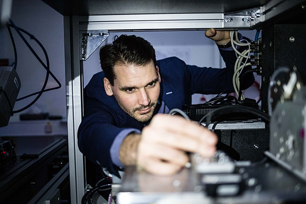
Hugh Simons sets up a sample on beamline ID06. Credits: Etienne Bouy. |
Simons and colleagues were surprised by the results: they discovered that the strain from these defects breaks the symmetry in the domain walls over several micrometres and drastically alters the material’s response to the applied electric fields. This also implies that the behaviour of the material is fundamentally affected by heterogeneities deep within the bulk material. “You can’t assume your material has the structure you think it has”, says Simons. “Our results conflict with 50 years of research”, says Simons. “These results will now have to be taken into account when designing and simulating these materials”.
A technique for the future EBS
Simons has been working alongside Carsten Detlefs, beamline responsible for ID06, developing the technique of Dark X-ray microscopy for the last four years. Together they have published various publications on the technique and some fundamental studies in metals.
This technique is new in synchrotrons and allows to study materials at different scales. Unlike bright field microscopy, where the sample is seen on a bright background, dark field microscopy detects only light that is scattered by the sample, not from direct illumination. In case of dark-field x-ray microscopy, the signal originates from Bragg diffraction. This new technique is therefore ideal for crystalline materials like most metals, ceramics, rocks, ice, semiconductors, etc. Many physical and mechanical properties of these materials depend on their internal structure, organised into grains of different sizes. Dark-field X-ray microscopy is a non-destructive technique which allows 3D mapping of orientations and stresses from 100 nanometres to 1 millimetre. The technique allows zooming in and out in both direct and angular space.
Carsten Detlefs explains that “Dark field x-ray microscopy is inspired by dark-field transmission electron microscopy (TEM). It combines elements from x-ray diffraction topography, x-ray tomography and x-ray microscopy. Compared to TEM, we have a much better angular resolution, although a not as good spatial resolution. What is more important, however, is that we can look inside the material, whether it is inside a furnace or other sample environment, and see how the sample evolves during processing”.
The new beamline which will feature this technique will be ready in 5 years’ time. However, the ID06 has become the launching platform for it. “It is very impressive to see movies of how the internal structure changes to such a detail. We are going where no one has ever gone before”, says Simons.
Reference:
Simons, H. et al, Nature Materials, 25 June 2018. DOI: 10.1038/s41563-018-0116-3.
Text by Montserrat Capellas Espuny
Top image: Dark-field x-ray microscopy enables coinciding maps of lattice strain (top), lattice orientation (middle) and diffracted intensity (bottom) - all from a single buried grain in the bulk material. Credits: Hugh Simons.


