- Home
- News
- General News
- Quantifying the...
Quantifying the quantum dot
25-02-2009
Researchers use X-ray measurements at the ESRF to characterise home-grown semi-conductor nanostructures – their unique methodology is documented in Physics Review Letters (PRL)
Share
The modern world of technology is built on sand. Or more accurately, crushed quartz, which is an abundant source of the silicon commonly used to make LEDs, photovoltaic cells, and the famous microprocessor: all appearing in increasing amounts of products such as laptops, mobile phone chargers, and even the latest Nike trainers. Silicon is a semi-conductor, which means that electrons can travel through it, but they need an extra input of energy, transferred by a photon, to do so. Semiconductor devices are thus great at turning photons (light) into moving electrons (current), as in a photovoltaic cell, or vice versa in an LED. But these devices could be improved, and there are high hopes for doing this with a semiconductor device so small it becomes ‘zero-dimensional’ - a quantum dot.
The amount of energy an electron has in either its free-travelling state or its ground state varies depending on the structure and composition of the material it is moving through. Electrons will occupy the lowest energy level possible, so if there is a small area with a lower ground state, energy electrons will migrate there. If the low energy region is small enough, (a few hundred atoms across or less) electrons trapped there will be very densely packed, interacting often and energetically. This is the technology called a ‘quantum dot’, and in practical terms, they could be used in super-bright LEDs, or possibly high-efficiency photovoltaic cells. The challenge now is to characterise the nature of the dense knot of electrons, which is intimately related to the sizes, composition of and energy levels within the low-energy islands they occupy.
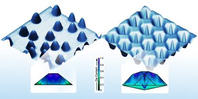
A team of scientists from the Commissariat à la Énergie Atomique (France), the ESRF, the University of Milano-Bicocca (Italy) and the Johannes Kepler Universität Linz (Austria) grew quantum-size islands of germanium on a silicon bottom layer that had been partly pre-patterned with pits (shown in illustration). Taking X-ray diffraction patterns of both sets of islands, those in silicon hollows and those grown on a flat surface, allowed the two structures to be compared without losing their complexity. For instance, although initially the silicon and germanium atoms occupy different regions, the temperatures at which the islands are fabricated allows the atoms to keep moving around once the structure is laid down, leading to an uneven mixture of elements within each island. Another advanced feature is the strain in the system – although both silicon and germanium form crystal lattices, these lattices aren’t the same size. When one is grown on top of the other, both get squeezed a bit – but the squeezing isn’t the same for islands grown in pits or on the flat, or constant within any individual island.
X-rays give the best resolution data available on chemical composition and inter-atomic distances, from which the deformation, strain and composition within the island can be found, but they do not image the nanostructures directly. For a real-space idea of what is going on, you have to turn to a theoretical model. In their recent PRL paper, the group of researchers present their success in joining the dots between the x-ray results and the numerical simulations, and derive a real-space model of the nanostructures that could not be achieved by either method alone. A cross-section through these models is shown inset into the accompanying illustration, colour-coded according to composition.
Tobias Schülli, lead author on the paper, explained it in these terms: “Theory can very well describe structures in their equilibrium states; but structures grown in this way are not in equilibrium. Microscopy sees only the external shape of the island, while x-ray light sees atomic distances and chemical composition. What’s needed is a combined approach, where theorists build an island in their computer, and iterate their simulation until it fits the ‘blurred image’ derived from the experimental data. When we look at this blurred image through the lens of the theory, we get a quite detailed image of the islands' interior.”
Using this lens, they have explained how the strain energy of germanium islands depends on the silicon patterning of the substrate. This gives a way of tuning the energy levels of a quantum dot, and therefore the wavelength of light it will interact with, while simultaneously pinning down their specific location and controlling their size – in essence, quantifying the quantum dot.
Reference:
T. Schülli et al., Phys. Rev. Lett., 102, 025502 (2009)
Top image: Germanium islands formed in silicon pits - with detail of internal composition


