- Home
- News
- Spotlight on Science
- Innovative resistive...
Innovative resistive memories studied by hard X-ray photoelectron spectroscopy (HAXPES)
31-05-2010
Resistive memories are candidates for future non volatile random access memories (RAMs). Their functioning is based on the ability to switch between high and low resistance states. However, the physical mechanism responsible for the low resistivity remains a mystery. Now a team of scientists from the CEA Grenoble and the ESRF have performed non-destructive HAXPES measurements on a NiO device before and after resistive switching. Their results suggest that conduction occurs via defects such as oxygen vacancies.
Share
Resistive RAMs (RRAM)s are interesting candidates for the next generation of non-volatile memories in terms of data retention, low power consumption and scalability. The RRAM-data storage principle is based on switching the resistivity between high (“OFF”) and low (“ON”) resistance states. Different mechanisms are currently being investigated to change the resistivity of a specific material sandwiched between two metallic electrodes.
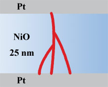
For the Oxide RRAM (OxRRAM), voltage or current pulses are applied to a transition metal oxide. The formation and rupture of a conductive filament (cf. Figure 1) through the oxide is suggested to explain the resistive switching. However, the conduction mechanism and the characteristics of the filaments are still poorly understood. Further information concerning the structure, size and chemical composition of these filaments are needed to efficiently control and optimise the resistive switching behaviour of RRAM.
 |
|
Figure 1. Geometry of the OxRRAM memory cell. |
HAXPES was carried out at beamline ID32 to provide a better understanding of the switching mechanism. Investigation of chemical states with depth sensitivity was performed in a non destructive way by using energies of 2.1, 6.5 and 9.75 keV thus tuning the sampling depth from about 7 to 30 nm. Spectra were recorded for the high and low resistance states on the same samples. The low resistance state was prepared ex situ (without top electrode) by applying positive (+8 V) and negative (-8 V) voltages to the NiO surface. The Ni 2p, O 1s and Pt 4f core levels were investigated to detect possible chemical changes after commutation.
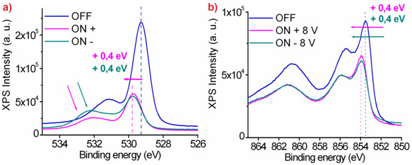
Figure 2 shows the O 1s and Ni 2p core levels measured at 2.1 keV (sampling depth ≈ 7 nm). A shift of 0.4 eV towards higher binding energies is observed for both the positive and negative voltages, compared to the spectrum for the OFF state. This is attributed to defects, such as O vacancies that might be created during the commutation. The resulting band gap states induce a band shift throught the NiO layer. Two main contributions are identified on the O 1s spectra and assigned to: a) ionic bonds of NiO (O2- - Ni2+) at 529.4 eV, b) O2- bonded to Ni3+ or O- bonded to Ni2+ at 531.5 eV. The ratio between these two components changes after commutation with an increase of the second contribution.
 |
|
Figure 2. Core level spectra obtained at 2.1 keV before and after electrical switching for a) O 1s and b) Ni 2p. |
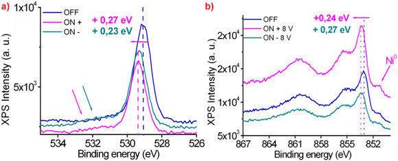
Roughly tripling the sampling depth (> 20 nm), and measuring the O 1s spectra at 9.75 keV (see Figure 3) again an increase of the second component is observed and attributed to defects such as Ni vacancies. However, regarding the Ni 2p spectra measured at this energy, an additional component related to Ni0 appears at lower binding energies. This proves the presence of Ni in the metallic state near the bottom NiO/Pt interface, whatever the resistive state of the memory cell. No increase in the Ni0 component is observed after resistive switching. This indicates that the formation of the conductive filaments is not related to metallic nickel but to defects such as oxygen vacancies. This is the first evidence of the major role of such vacancies and is an important step towards the understanding and further development of this new class of nano-devices.
 |
|
Figure 3. Core level spectra obtained at 9.75 keV before and after electrical switching for a) O 1s and b) Ni 2p. |
Authors
P. Calka (a) , E. Martinez (a), C. Guedj (a), D. Lafond (a), P. Bayle-Guillemaud (b), B. Detlefs (c), J. Roy (c), J. Zegenhagen (c)
(a) CEA, LETI, MINATEC, Grenoble (France)
(b) CEA, INAC, SPEM, Grenoble (France)
(c) ESRF
Top image: Sketch depicting a conductive filament within an OxRRAM.


