- Home
- News
- Spotlight on Science
- Shedding light on...
Shedding light on the heart of a transistor
26-07-2011
X-ray nanobeam diffraction was used to explore the heart of a fully processed field-effect transistor. The structural and strain properties of a single SiGe island and the overlying strained Si channel, which represents the active area of the device, were investigated with a beam focused to a diameter of 400 nm. This is pioneering work in the application of X-ray diffraction as a local probe for the study of functional devices.
Share
Coplanar X-ray diffraction is a well-established, powerful tool to determine the structural properties of various materials. The absence of specific requirements for the preparation of the sample has made it one of the most prominent methods in material science both to quickly check the sample quality and to gain crucial information about new materials. A limiting factor for nanoscale materials is the lack of spatial resolution, as the beams used for probing the sample are usually in the range of mm down to a few tens of micrometres. We used the latest advances in technology related to hard X-ray focusing and the precise sample positioning available at ID01, the ESRF beamline for anomalous scattering, to explore the centre of a fully-processed transistor device, an area of a size well below one micrometre.
The device investigated was a so called 'dot-FET' [1], a field-effect transistor with a strained Si channel as its main active element. A common approach to enhance transistor device properties such as carrier mobility and switching speed is to apply strain to the active channel. Tensile strain improves electron mobility in n-type transistors while compressive strain is used for a better hole mobility in p-type devices. In the case presented here the transistor is n-type. Due to the similarity of the crystal structures of Si and Ge and a lattice mismatch of 4.2%, a buried Ge layer can be used to apply tensile strain to the Si channel. With planar SiGe structures, which are commonly used as stressor in such devices, problems arise because such a 2D layer cannot relax properly and dislocations and other defects are easily developed, corrupting the functionality of the device. In this device, the structure used to apply strain to the Si channel is an epitaxially grown 3D SiGe island with 250 nm diameter and about 50 nm height. Due to its enhanced relaxation, more Ge can be incorporated into the stressor without introducing defects. To easily locate the islands for the successive processing steps in transistor fabrication, they are grown on pre-patterned Si (001), as the transistor needs to be centered with high precision around a selected island (see Figure 1 a-d) [2]. The islands are then overgrown with a Si capping layer that finally acts as a channel in the transistor. In the completed device, this small active area is buried underneath several layers such as the gate stack and metal contacts, which makes it hard to assess the transistors structural properties while preserving its functionality.
 |
|
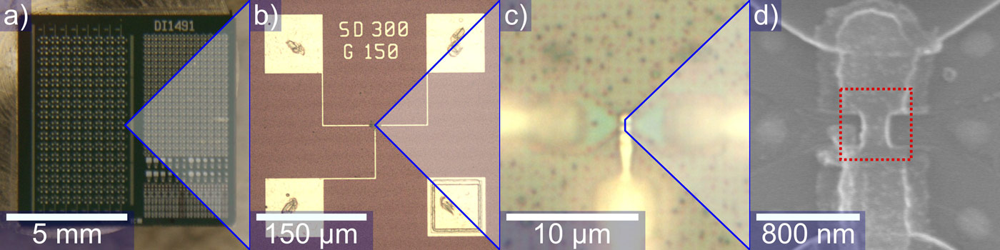
Figure 1. Photograph (a) and optical micrographs (b, c) of the investigated sample at different scales. The Si substrate of size 9 mm x 9 mm with numerous devices processed on it can be measured without any sample preparation, leaving the devices in their functioning state. (d) shows a SEM image of a transistor sample after the formation of the gate finger, before source and drain contacts are in place. The transistor is precisely aligned on the patterned array of SiGe islands (lateral island period: 800 nm). The red square marks the area probed by the X-ray beam. |
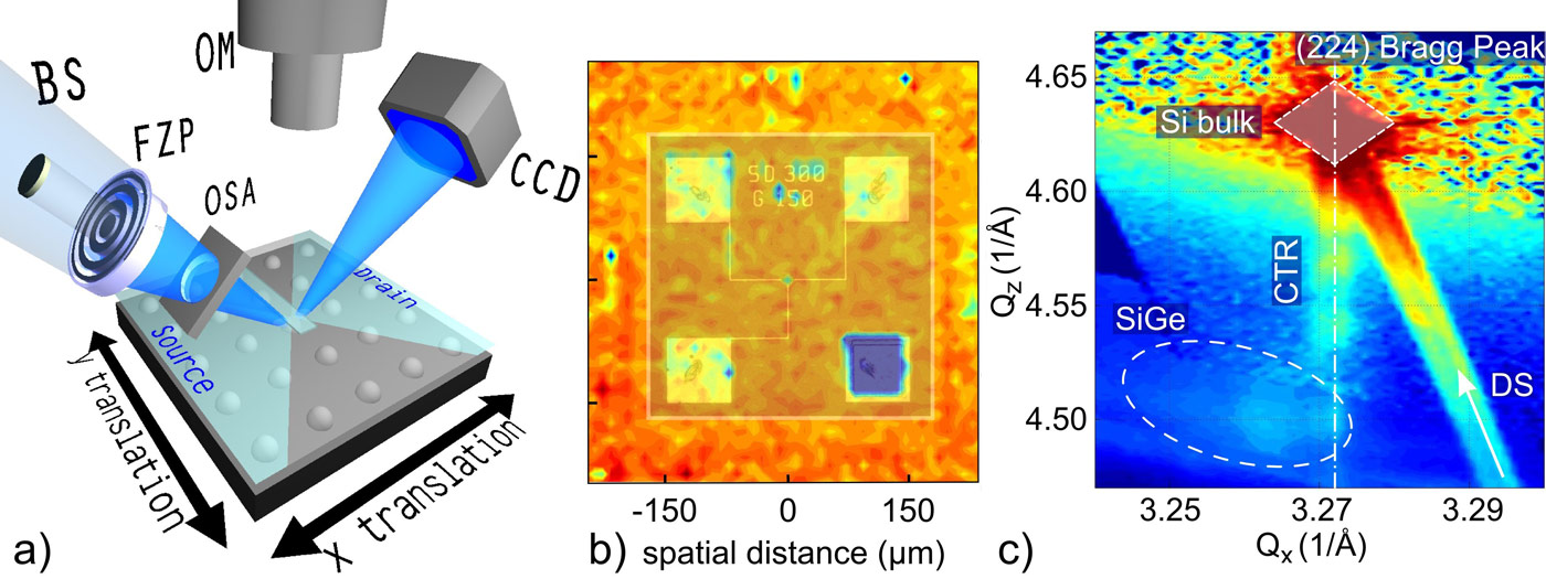
X-ray diffraction with a beam focused to a diameter of several hundred nanometres can be used to probe exclusively this small area. The setup for focusing hard X-ray beams currently available at beamline ID01 is shown in Figure 2a. By scanning the sample in both real (Figure 2b) and reciprocal space (Figure 2c), we were able to identify the specific island at the core of the transistor and record reciprocal space maps to determine the strain properties of both the island and the Si channel. From this measurement we can derive valuable information such as the average Ge content of the SiGe island or the thickness of the capping layer (cf, Figure 2c). The latter was found to be smaller than its initial value, due to device processing steps like etching, implanting and annealing. In our case the thickness of the Si channel was reduced from 30 nm, measured in the as-grown sample, to about 24 nm in the completed device. Combining the information we obtained from the XRD measurements with finite element simulations, we discovered that tensile strain values of 1% are achieved in the Si channel along the source-drain direction which are locally reduced due to the influence of the gate stack.
 |
|
Figure 2. a) Setup used at ID01: a beamstop (BS), a Fresnel zone plate (FZP) and an order sorting aperture (OSA) are used to focus the incoming X-ray beam. An optical microscope (OM) is used for rough sample alignment; the exact positioning is done through the X-ray beam itself by scanning the sample position while the goniometer is tuned to a characteristic signal, e.g. a Si Bragg peak, or the diffuse SiGe signal. The attenuation of this signal by metal contacts can be used to determine the position of the SiGe island in the centre of the transistor. b) An X-ray diffraction scanning (SDX) map is shown overlaid with a transparent microscope image as guide to the eye. c) Reciprocal space map including the Si (224) Bragg peak and the diffuse signal from the SiGe island. From the position of this signal in reciprocal space an average Ge content can be determined; the crystal truncation rod (CTR) gives us information on the thickness of the Si channel. The detector streak (DS) arises due to enhanced air scattering when the goniometer passes through the intense Si Bragg peak. |
These investigations are highly valuable for the development of process flows, as samples from different processing steps can be compared without interference from preparation for analysis. Furthermore, even the investigation of devices during operation is feasible, which is important e.g. for aging and reliability studies.
Principal publication and authors
X-ray nanodiffraction on a single SiGe quantum dot inside a functioning field-effect transistor, N. Hrauda (a), J.J. Zhang (a,b) , E. Wintersberger (a,c), T. Etzelstorfer (a), B. Mandl (a), J. Stangl (a), D. Carbone (d), V. Holý (e), V. Jovanović (f,g), C. Biasotto (f,h), L.K. Nanver (f), J. Moers (i), D. Grützmacher (i) and G. Bauer (a), Nano Lett. 11, 2875–2880 (2011).
(a) Institute for Semiconductor Physics, JKU Linz (Austria)
(b) IFW Dresden (Germany)
(c) HASYLAB at DESY, Hamburg (Germany)
(d) ESRF
(e) Faculty of Mathematics and Physics, Charles University Prague, Praha (Czech Republic)
(f) DIMES, TU Delft (The Netherlands)
(g) FER, University of Zagreb (Croatia)
(h) CCS, State University of Campinas, São Paulo (Brazil)
(i) Halbleiter-Nanoelektronik (IBN-1) Forschungszentrum Jülich GmbH (Germany)
References
[1] O.G. Schmidt, K. Eberl, IEEE Transactions on Electron Devices 48, 1175 (2001).
[2] V. Jovanović, C. Biasotto, L.K. Nanver, J. Moers, D. Grützmacher, J. Gerharz, G. Mussler, J. van der Cingel, J.J. Zhang, G. Bauer, O.G. Schmidt, L. Miglio, IEEE Electron Device Letters 31, 1083–1085 (2010).
Top image: Shedding light on the heart of a transistor.
partners


European Synchrotron Radiation Facility - 71, avenue des Martyrs, CS 40220, 38043 Grenoble Cedex 9, France.