- Home
- News
- Spotlight on Science
- Strong inside, weak...
Strong inside, weak outside: Graphene on Ir(111)
28-10-2011
Graphene, a single monolayer of carbon, features a set of fascinating properties. In particular, it has the largest tensile strength ever measured. Experiments at the ESRF now show that this large internal strength is in stark contrast to its weak bonding to the outside world, specifically to selected metal surfaces on which graphene can be produced by epitaxial growth.
Share
Graphene is created each time one sketches with a pencil. It is a single layer from the many layers that form the mineral graphite. In such a graphene sheet, carbon atoms are joined together in a strictly two dimensional structure, where every atom has three in-plane neighbours and a honeycomb mesh results. Graphite, in turn, is formed when graphene layers are stacked on top of each other in the right registry. Of course, much of the graphite debris left in a pencil trace will be much thicker than just one atomic layer, but inevitably, at some places, just one layer — graphene — can be found. This concept was exploited by A. Geim and K. Novoselov in order to produce graphene, which allowed demonstration of its unique electronic properties, i.e. the photon-like behaviour of the charge carriers, and earned them the Nobel Prize in physics in 2010.
A technologically more relevant process for producing graphene is its epitaxial growth on metal surfaces, yielding large, well-ordered films [1], see Figure 1. Therefore, it is important to determine whether the presence of the metal substrate disturbs the special properties of graphene, and whether it is possible to harvest graphene from its support for further processing. The strength of the binding between graphene and its host is crucial in both cases. A fingerprint of this bond strength can be found in the distance between the carbon sheet and the metal surface. However, this quantity is hard to determine accurately, likewise by experiment or theory, mainly because the graphene covers the surface like a carpet and thus large unit cells need to be considered. Furthermore, carbon is a weak scatterer for X-rays, the most sensitive structural probe. Regarding theory, on top of handling a large unit cell, the significant non-local van der Waals (vdW) interaction needs to be included, which is not standard in density functional theory (DFT) calculations.
 |
Figure 1. Scanning tunnelling microscopy (STM) image of graphene on Ir(111). The small dark spots are the centres of individual carbon rings. The large-scale superstructure is a moiré pattern which results from the superposition of the graphene lattice with the lattice of the metal surface underneath. On the lower left the honey comb structure of graphene is visualised by white lines. The image size is 15 nm × 15 nm. |
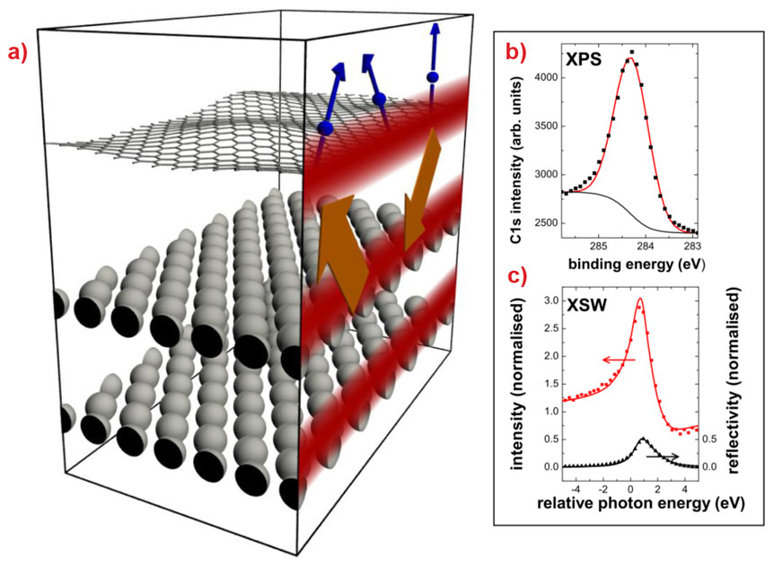
To facilitate a precise measurement of the height distribution of the carbon atoms in graphene on Ir(111), we performed an X-ray standing wave (XSW) analysis at beamline ID32. An X-ray standing wave is created in the interface region of a crystal using Bragg reflection (see Figure 2a). The maxima of the XSW, which are periodic with the Ir (111) lattice planes, are shifted inward by half the lattice plane distance when scanning through the Bragg reflection by changing the beam energy. Atoms exposed to the maximum of the standing wave field are strongly photo-excited. Therefore, scanning the XSW field and monitoring the photoelectron signal allows the (average) height of the carbon atoms above the surface to be determined. For graphene on Ir(111), we found a large mean height of the carbon atoms of h = (0.338 ± 0.004) nm from the change of the intensity of the C1s photo emission (Figure 2b) when scanning through the Ir(111) Bragg reflection (Figure 2c). This value is similar to the interlayer distance in graphite (0.336 nm), which is proof of the weak surface bonding.
 |
|
Figure 2. a) Schematic representation of the X-ray standing wave experiments. The corrugated honeycomb mesh represents graphene, on top of two Ir(111) lattice planes. Orange arrows: Interfering incoming and outgoing X-ray beam. Red stripes: Standing wave nodes. Blue spheres and arrows: Emitted photoelectrons. b) Squares: X-ray photoemission intensity of the C1s-peak. Thin line: Shirley-type background intensity, Thick line: Gaussian fit. c) X-ray reflectivity (triangles) and C1s photoemission yield during an XSW energy scan. |
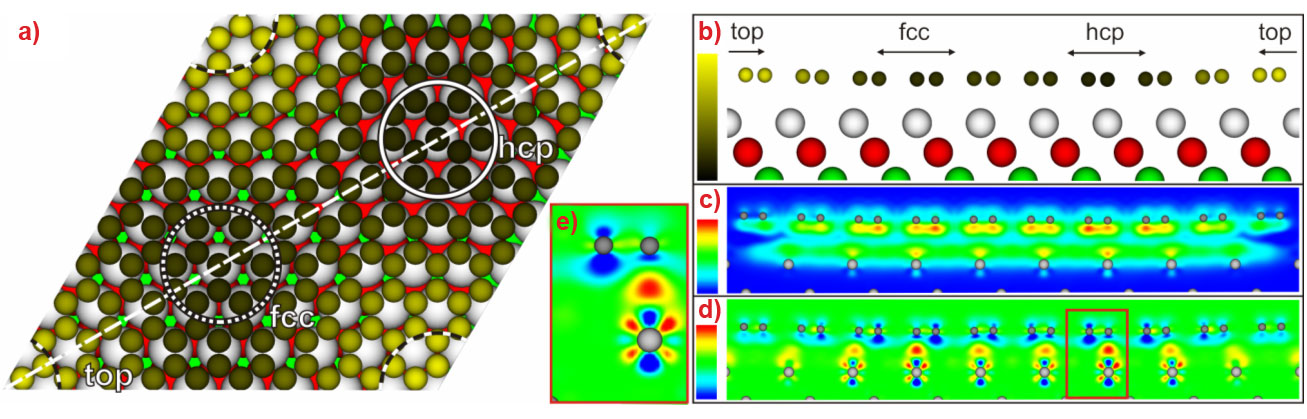
To complement these experimental results, we performed ab initio DFT calculations including the vdW interaction. The calculated mean value h = 0.341 nm is in good agreement with the experimental results. In addition, the calculation also reproduces the corrugated shape of graphene observed in STM, see Figure 3. Without going into detail, this is also in quantitative agreement with the XSW data. The variation in height is accompanied by a variation in bond strength. This becomes obvious in studies of the charge transfer caused by adsorption, visualised in Figure 2 (d and e). In special areas of the supercell, a small charge transfer takes place that leads to a charge accumulation at the graphene/Ir(111) interface. This indicates the formation of local bonding with weak covalent character. In addition, a globally attractive van der Waals interaction is present (spatial distribution visualised in Figure 2c), which is the dominating interaction in this system. The overall average binding energy found in our calculations is rather small, Eb = -50 meV/C, again similar to the corresponding value for graphite.
 |
|
Figure 3. a) Top view and b) side view (cut along the dashed line in (a)) of the relaxed geometrical structure of graphene/Ir(111) obtained by DFT including vdW interaction. The different regions (fcc, hcp, top) are marked by circles (a) or arrows (b-d). The colour scale indicated in (b) ranges from h = 3.20 Å (dark) to h = 3.65 Å (yellow). c) Real space visualisation of the nonlocal (i.e. vdW) binding-energy density caused by adsorption (blue: zero density, red: maximum density). d) The charge transfer upon adsorption (blue: charge depletion, red: charge accumulation). e) Magnified view in the hcp region (see red box in (d)). |
In summary, the binding of graphene in this specific system is weak and consequently the special electronic structure of graphene is maintained [2]. Further experiments have shown that it is possible to exfoliate the carbon film from its support for subsequent studies.
Principal publication and authors
C. Busse (a), P. Lazić (b), R. Djemour (a), J. Coraux (c), T. Gerber (a), N. Atodiresei (b), V. Caciuc (b), R. Brako (d), A.T. N’Diaye (a), S. Blügel (b), J. Zegenhagen (e), T. Michely (a), Graphene on Ir(111): Physisorption with Chemical Modulation, Phys. Rev. Lett. 107, 036101 (2011).
(a) I. Physikalisches Institut, Universität zu Köln (Germany)
(b) Peter Grünberg Institut (PGI) and Institute for Advanced Simulation (IAS), Forschungszentrum Jülich and JARA, Jülich (Germany)
(c) Institut Neél, CNRS-UJF, Grenoble (France)
(d) Ruđer Bošković Institute, Zagreb (Croatia)
(e) ESRF
References
[1] J. Coraux, A.T. N'Diaye, C. Busse and T. Michely, Nano Lett. 8, 565 (2008).
[2] I. Pletikosić, M. Kralj, P. Pervan, R. Brako, J. Coraux, A.T. N'Diaye, C. Busse and T. Michely, Phys. Rev. Lett. 102, 056808 (2009).
Top image: Graphene grown on top of a metal surface shows strong internal bonding, but only weak interaction with the substrate.
partners


European Synchrotron Radiation Facility - 71, avenue des Martyrs, CS 40220, 38043 Grenoble Cedex 9, France.