- Home
- News
- Spotlight on Science
- Anisotropic conductance...
Anisotropic conductance at interfacial domain walls in multiferroics
16-05-2012
The electrical conductance at the interfacial ferroelectric domain walls in hexagonal ErMnO3 is a continuous function of the domain wall orientation. A combination of experiments and theoretical studies reveal this phenomenon and its connection to the unexpected stability of head-to-head and tail-to-tail ferroelectric domain walls.
Share
Multiferroic materials are a likely source for novel domain and domain-wall properties as these systems often have unconventional mechanisms driving their spontaneous ordering. An unexpectedly high local electrical conductance has been measured at ferroelectric domain walls in BiFeO3 [1], whereas the 180° domain walls in hexagonal YMnO3 were found to have higher resistivity than the bulk material [2]. In the latter case, the primary symmetry-lowering order parameter is a unit-cell-tripling distortive mode and the subsequent geometrically-driven ferroelectricity is improper [3]. The tripling mode sets the orientation of the resulting spontaneous polarisation, which gives rise to an unusual distribution of ferroelectric domains [2,4]. This mechanism was also shown to have a remarkable impact on the electronic properties of the domain walls of hexagonal ErMnO3. In the present investigation, we have studied ErMnO3. Similar behaviour can be expected for the other members of the manganite series.
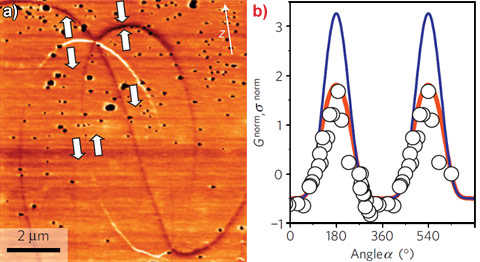
Samples of ErMnO3 were investigated by conductive atomic force microscopy (c-AFM) and piezo-response force microscopy (PFM) at ambient conditions. Figure 1a shows two intersections of six domains with in-plane spontaneous polarisation characteristic of this family of multiferroics [2,4]. The brightness of the c-AFM signal along the domain walls reveals that these walls have non-trivial orientation-dependent conductance properties. The highest conductance is found at walls where the electric polarisation meets tail-to-tail, while the lowest conductance is observed at walls in the head-to-head polarisation configuration. Figure 1b shows the angular dependence of the normalised local conductance Gnorm, which exhibits a distinctly nonlinear relationship between the orientation and the conductance of the domain wall.
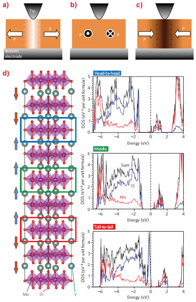
This dependence can be understood using the schematics and density functional calculations in Figure 2. At tail-to-tail domain walls (Figure 2a), the adjacent bound negative charge layers cause an energetically costly divergence in electrostatic potential that must be ameliorated by the accumulation of positive charge. This can be achieved using the readily available mobile hole carriers since the system is a p-type semiconductor. At the same time, the variation in electrostatic potential shifts the Fermi level at the tail-to-tail walls into the broad O(2p)-Mn(3d) valence band, where the carrier effective mass is low and the corresponding hole mobility is high. In contrast, at head-to-head walls (Figure 2c), the bound positive charge layers require negative charge for screening. But because free negative charges (electrons) are scarce in a p-type semiconductor, screening can only be achieved by bound charges such as cation vacancies, which do not contribute to the conduction. At parallel domain walls there is no polar discontinuity and the background conductance of the system is expected (Figure 2b).
 |
|
Figure 2. a-c) Schematic illustrations showing tail-to-tail, side-by-side, and head-to-head domain walls respectively, where + and - indicate positive and negative bound charges at the domain wall. d) Calculated local density of states (black lines) in the head-to-head (upper right), tail-to-tail (lower right) and domain-centre (middle right) regions of the YMnO3 supercell shown on the left. Blue and red lines show oxygen and manganese contributions respectively. |
To make a closer connection with the experimental data, the equilibrium model described in [5] has been taken as starting point. This model predicts an orientation-dependent spatial distribution of conductivity around charged domain walls in semiconductors. It was found, however, that to reproduce the experimental data one needs to go beyond the calculation of the equilibrium conductivity σDW, and instead calculate the conductance G, based on the actual, non-equilibrium flow of current from the expanded c-AFM tip through the sample, both inside and outside of the region defining the domain wall. This calculation gives the conductance G(α) = σDW (α) / {1 + [2r/w(α)] ln [(σDW (α) + σbulk )/ σbulk ] }, where σbulk is the bulk conductivity and r/w(α) is the ratio between the radius of the c-AFM tip and the effective orientation-dependent width w(α) of the domain wall as determined by the accumulation or depletion of holes. This formula reproduces the measured data points in Figure 1 in a strikingly accurate way (red curve in Figure 1b).
In summary, it has been demonstrated that the conductance at ferroelectric domain walls in hexagonal ErMnO3 varies continuously with the orientation of the wall. The variation of the conductance by an order of magnitude is the combined consequence of carrier accumulation and local changes in band-structure. Both of these effects have been derived theoretically, using phenomenological electrostatic and ab initio density functional theory, respectively. In conventional ferroelectrics such energetically unfavourable head-to-head and tail-to-tail domain walls are usually avoided. However, their presence is enforced in ErMnO3 because of the protected topology of intersecting domain states in hexagonal manganites [2,4]. As ferroelectric domain walls can be routinely modified using electric fields, these results suggest a new degree of flexibility for domain boundary engineering and oxide-based devices in which interfaces can be dynamically modified even after assembly into a device architecture.
Principal publication and authors
Anisotropic conductance at improper ferroelectric domain walls, D. Meier (a,b), J. Seidel (a,c,d), A. Cano (e), K. Delaney (f), Y. Kumagai (g), M. Mostovoy (h), N.A. Spaldin (g), R. Ramesh (a,b,c) and M. Fiebig (g), Nature Materials 11, 284–288 (2012).
(a) Department of Physics, University of California, Berkeley (USA)
(b) Department of Materials Science and Engineering, University of California, Berkeley (USA)
(c) Materials Sciences Division, Lawrence Berkeley National Laboratory, California (USA)
(d) School of Materials Science and Engineering, University of New South Wales, Sydney (Australia)
(e) ESRF
(f) Materials Research Laboratory, University of California, Santa Barbara (USA)
(g) Department of Materials, ETH Zürich (Switzerland)
(f) Zernike Institute for Advanced Materials, University of Groningen (The Netherlands)
References
[1] J. Seidel et al., Nature Mater. 8, 229-234 (2009); S. Farokhipoor and B. Noheda, Phys. Rev. Lett. 107, 127601 (2011).
[2] T. Choi et al., Nature Mater. 9, 253-258 (2010).
[3] C.J. Fennie, K.M. Rabe, Phys. Rev. B 72, 100103 (2005); B.B. Van Aken, T.T.M. Palstra, A. Filippetti, and A.N. Spaldin, Nature Mater. 3, 164-170 (2004).
[4] T. Jungk, Á. Hoffmann, E. Soergel and M. Fiebig, Appl. Phys. Lett. 97, 012904 (2010).
[5] E.A. Eliseev, A.N. Morozovska, G.S. Svechnikov, V. Gopalan and V.Y. Shur, Phys. Rev. B 83, 235313 (2011).
Top image: c-AFM image of ErMnO3 on a surface with in-plane electric polarisations indicated by arrows.


