- Home
- Industry
- Industry news
- Observing defects...
Observing defects in diamonds
20-04-2021
The ESRF’s state-of-the-art topography or “X-ray diffraction rocking-curve imaging” facility has been exploited in the Horizon 2020 “Green Diamond” project to analyse the quality of artificially grown diamonds to be used in high power electronics - key components for future efficient green electricity transmission.
Share
Defects in crystalline materials can have a dramatic impact on the performance of devices using those materials. The ESRF’s synchrotron X-rays provide a unique method for rapid mapping of defects in crystalline materials.
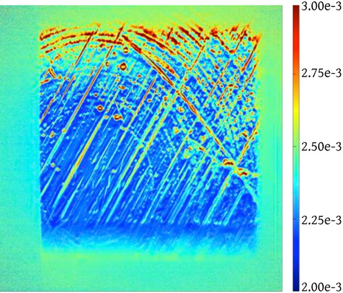
In the Green Diamond project, synchrotron X-ray topography maps were recorded for diamond substrates to show defect density distribution and the coordinates of severe defect locations of primarily bulk-to-surface defects. This was an essential prerequisite to correlate the relationship between the location of these defects and their impact on the performance of diode and transistor devices.
The ESRF’s monochromatic beam X-ray diffraction rocking-curve imaging instrument BM05 was employed using a novel methodology that is unique to the ESRF. This method enabled depth-profiling measurements of the quality of the near surface layer of substrates, the crystal-structure quality of CVD grown doped diamond epi-layers and defects at the epi-to-substrate interface. The resulting mapping of the diamonds showed clearly that the epilayer quality depends strongly on the quality of substrate and moreover the quality of treated surface.
For further information: Diamonds have a glittering future in green energy production
Top image: Beamline BM05


