- Home
- Users & Science
- Scientific Documentation
- ESRF Highlights
- ESRF Highlights 2000
- Microfocussing and Imaging
- Relaxation in Doped Strained Layers of Compound Semiconductors
Relaxation in Doped Strained Layers of Compound Semiconductors
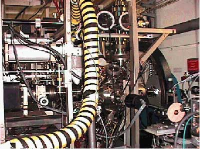
Strained layers of compound semiconductors such as InxGa1xAs grown epitaxially on the (001) surface of GaAs form the basis of optoelectronics devices on which the much of the modern communications industry is based. For such devices to operate reliably over extended periods, the strained layer must not relax by creation of misfit dislocations at the interface as these act as local heating and deformation sites. Using a purpose-built molecular beam epitaxy reactor (Figure 107), now installed on beamline BM5 of the ESRF, high-resolution X-ray diffraction topography (imaging) has been used to observe in situ, the nucleation and propagation of the very first misfit dislocations in fully-strained epilayers of In0.04Ga0.96As on (001) GaAs. As doping bulk crystals results in pinning of dislocations, analogous experiments were performed to try to suppress the motion of misfit dislocations and hence raise the critical thickness at which strained epitaxial layers relax.
 |
Fig. 107: The in situ molecular beam epitaxy reactor installed on beamline BM5.
|
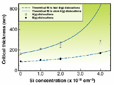
Relaxation is initially anisotropic and this is associated with the two types of dislocation found in the zincblende structure. The fast B(g) dislocations, running in the [110] direction, are nucleated before the slow A(g) set, running in the orthogonal [![]() 10] direction. On doping with Si up to a maximum concentration of 4 x 10¹⁸ atoms/cm3, an increase in critical thickness was observed for both dislocation sets. For the highest concentration, no slow A(g) dislocations were observed up to the greatest thickness grown.
10] direction. On doping with Si up to a maximum concentration of 4 x 10¹⁸ atoms/cm3, an increase in critical thickness was observed for both dislocation sets. For the highest concentration, no slow A(g) dislocations were observed up to the greatest thickness grown.
When a dislocation in the substrate crosses into the strained layer, there is a lateral force on the segment in the epilayer as a result of the biaxial strain present. As a consequence, the segment glides on an inclined slip plane, leaving behind the misfit dislocation segment at the interface. The line tension of the misfit segment results in a retarding force on the threading segment. In equilibrium, these are equal and this results in the classic Matthews-Blakeslee [1] equation for the critical thickness at which misfit dislocations are formed. The Matthews-Blakeslee model has been extended to include an anisotropic Peierls lattice friction and a further frictional force varying linearly with the dopant concentration. There is a very satisfactory agreement between the extended model and experiment (Figure 108). Substantial lattice friction is present in the undoped samples for both dislocation sets and the increase in frictional force with dopant concentration is the same for both fast and slow dislocations.
 |
Fig. 108: Variation of the critical thickness with silicon concentration. The curves are fits to the modified Matthews-Blakeslee model.
|
A small change was observed in the critical thickness as a function of growth temperature. Inclusion of a temperature dependent term in the Matthews-Blakeslee model enabled an activation energy 0.3 ± 0.2 eV to be determined for the undoped layers. This value, which is consistent with the observation of enhanced misfit dislocation mobility, is lower than measured previously and probably arises from the improved vacuum conditions and elimination of the long growth pauses necessary to expose the photographic plates at the less intense Daresbury SRS.
The ESRF experiments not only show that the Matthews-Blakeslee model is capable of being extended successfully but also show that the critical thickness can be raised substantially by doping at levels that are consistent with device requirements.
Reference
[1] J.W. Matthews and A.E. Blakeslee, J. Crystal Growth 27 118 (1974).
Principal Publication and Authors
B.K. Tanner (a), P.J. Parbrook (b), C.R. Whitehouse (b), A.M. Keir (c), A.D. Johnson (c), J. Jones (c), D. Wallis (c), L.M. Smith (c), B. Lunn (d) and J.H.C. Hogg (d), Appl. Phys. Letts. 77, 2156-8 (2000).
(a) University of Durham (UK)
(b) University of Sheffield (UK)
(c) DERA. Great Malvern (UK)
(d) University of Hull (UK)


