- Home
- Users & Science
- Scientific Documentation
- ESRF Highlights
- ESRF Highlights 2000
- Microfocussing and Imaging
- In situ X-ray Microscopic Study of Electromigration
In situ X-ray Microscopic Study of Electromigration
The interconnect structures in modern microelectronic devices are currently 500 nm wide and operate at very high current densities of nearly 106 A/cm2 without excessive Joule heating. At these current densities one of the major failure mechanisms is electromigration (EM), i.e. the transport of atoms in a metallic interconnect along the direction of electron flow. The material transport can result in voids in the wire leading to open circuit failures as well as hillocks which extrude from the original interconnect causing short circuits. EM is one of the principal factors limiting microprocessor performance.
In a passivated interconnect the mass flow due to EM is constrained by encapsulation. This leads to a high mechanical stress in the interconnect which influences the material transport significantly. Therefore, EM should be studied in situ using an intact layer system including all barriers and passivation layers. For this purpose an imaging technique is required which maintains high spatial resolution when penetrating through several micrometres of dielectrics. Due to the high penetration power of X-rays through matter and the high spatial resolution, X-ray microscopy overcomes several limitations of conventional microscopic techniques. It utilises the natural absorption contrast between the elements of interest; i.e. Cu interconnects embedded in dielectrics.
 |
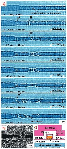
Fig. 119: a) A selection of the X-ray micrographs taken at a photon energy of 4 keV observing the mass transport by electromigration in a passivated Cu interconnect with 600 nm linewidth. b) SEM micrograph showing the stressed Cu interconnect after removal of the passivation layer by dry etching. c) Cross-section of the passivated Cu interconnect layer system used for the electromigration studies.
|
Using the full-field transmission X-ray microscope (TXM) installed at ID21 [1], we performed the first direct X-ray microscopic observation of an EM process. To visualise the dynamics of the EM, the sample (NIST test structure, ASTM standard F 1259M-96, Figure 119c) was stressed by increasing the current density from 0 up to 2 x 10⁷ A/cm2 during 131 minutes of observation. A sequence of 200 images - each with an exposure time of 30 s - was recorded with the TXM, displaying directly the dynamical transport of matter caused by EM. Selected X-ray micrographs of the transition region between the wide and the small part of the test structure at the cathode site are shown in Figure 119a. Initial damage of the interconnect was seen after a stress time of 5 minutes. Following this, self-healing effects (see Figure 119a, A ![]() A´ and B
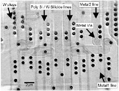
A´ and B ![]() B´) and formation of new voids was observed. Very fast and significant changes of the failure site in the last 10 minutes of the experiment show the effects of the rapidly increasing current density which is due to a decreasing cross-section of the interconnect. For comparison, a SEM micrograph is presented which shows the failure region of the stressed interconnect (Figure 119b) after removal of the passivation layers. Note that the final mass distribution, as detected by a standard failure analysis, cannot be related to the early stages of the EM process. In addition, the X-ray micrograph shown in Figure 120 demonstrates that intact microprocessor structures can be observed by employing the natural absorption contrast between elements. Details of the W plugs down to 70 nm size are resolved. The in situ observation of the EM and the microprocessor images reveal the potential of X-ray microscopy as an important new tool to study mass transport phenomena and to investigate failure mechanisms in electronic devices.
B´) and formation of new voids was observed. Very fast and significant changes of the failure site in the last 10 minutes of the experiment show the effects of the rapidly increasing current density which is due to a decreasing cross-section of the interconnect. For comparison, a SEM micrograph is presented which shows the failure region of the stressed interconnect (Figure 119b) after removal of the passivation layers. Note that the final mass distribution, as detected by a standard failure analysis, cannot be related to the early stages of the EM process. In addition, the X-ray micrograph shown in Figure 120 demonstrates that intact microprocessor structures can be observed by employing the natural absorption contrast between elements. Details of the W plugs down to 70 nm size are resolved. The in situ observation of the EM and the microprocessor images reveal the potential of X-ray microscopy as an important new tool to study mass transport phenomena and to investigate failure mechanisms in electronic devices.
 |
Fig. 120: X-ray micrograph of an intact integrated circuit with two AlCu metallisation layers and tungsten plugs connecting the levels.
|
Reference
[1] B. Kaulich, S. Oestreich, M. Salome, R. Barrett, J. Susini, T. Wilhein, E. DiFabrizio, M. Gentili and P. Charalambous, Appl. Phys. Lett. 75, 4061 (1999).
Principal Publication and Authors
G. Schneider (a), D. Hambach (b), B. Kaulich (c), N. Hoffmann (d), W. Hasse (d), K. Hoffmann (e), B. Niemann (b) and J. Susini (c), Appl. Phys. Lett., accepted for publication.
(a) Lawrence Berkeley National Laboratory (USA)
(b) Georg-August-Universität, Göttingen (Germany)
(c) ESRF
(d) Universität Hannover (Germany)
(e) Micronas GmbH, Freiburg (Germany)


