- Home
- Users & Science
- Scientific Documentation
- ESRF Highlights
- ESRF Highlights 2001
- Methods and Instrumentation
- Kirkpatrick-Baez Optics for Sub-Micrometre Focusing
Kirkpatrick-Baez Optics for Sub-Micrometre Focusing
Microanalysis covers an important area of research with synchrotron radiation. Its applications require the highest possible spatial resolution. The small source size (a few tens of micrometres) and low divergence (a few tens of micro-radians) of the X-ray beams produced by the ESRF storage ring provide excellent starting conditions to create small beams. Still high-performance X-ray optics are needed to demagnify the source by focusing it onto the sample under study. Many optical devices have been developed to concentrate X-ray beams to very small spots, sometimes even smaller than 100 nanometres.
Focusing methods based on reflection by curved surfaces coated with a single layer (mirror) or a stack of many layers (multilayer) present a number of advantages such as high irradiance gain, wide energy range, large acceptance, even at high energy with high efficiency. Here we want to report on a crossed mirror system that has been developed at the ESRF. It is based on the so-called Kirkpatrick-Baez (KB) design. Two orthogonal coated silicon substrates are bent into elliptical shapes by mechanisms based on flexure hinges. This device provides both very high accuracy and flexibility. It uses precise motors to tune the substrate shape to the experimental conditions such as focal distance and energy. Eight degrees of freedom are needed for alignment and focusing. The length of the substrates of the systems developed ranges from 92 to 300 mm. The surface quality of the substrates and the reading accuracies have to be very high. Typically, the final shape can be obtained to within a few nanometres. Novel figuring techniques will allow us to achieve a shape accuracy around 1 nanometre and maybe even below [1].
 |
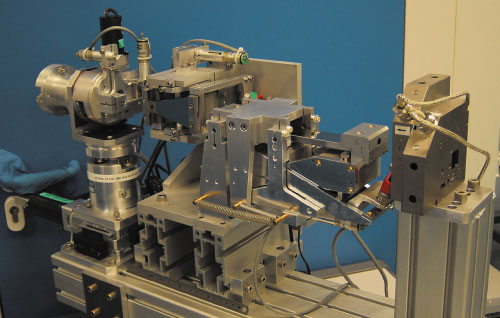
Fig. 163: Microfocusing Kirkpatrick-Baez setup. |
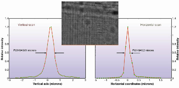
Figure 163 shows a specific setup studied on beamline ID19. At about 140 m from the source the dimensions of the monochromatic beam of 19 keV energy were defined by precise slits 0.2 mm x 0.25 mm wide. This beam was first reflected by a 170 mm long vertically focusing platinum coated mirror set at 3 milliradian grazing incidence. Then it was focused horizontally onto the sample by the 96 mm long second mirror. An X-ray sensitive CCD camera was used for computer-aided alignment of the mirrors with respect to the beam. A linear wavefront optimisation technique [2] served to shape the mirrors correctly. A 43 µm wide platinum stripe deposited on a polished silicon substrate set at a glancing angle of 2.8 milliradian was used as a very narrow reflective pseudo-slit, 0.12 µm wide, and scanned across the focus. The measured full widths at half maximum (FWHM) were 0.2 µm horizontal and 0.6 µm vertical (see Figure 164). These values were bigger than both the ideal source image and the diffraction-limited spot sizes of 48 by 65 nanometres. Vibrations were clearly identified as a major contribution to blurring. The irradiance gain was estimated to 3.5 x 10⁵.
 |
Fig. 164: Vertical and horizontal scans through the focus by a 0.12 micrometre width reflective slit. Inset: projection image of a gold grating with minimum periods of 300 nm. |
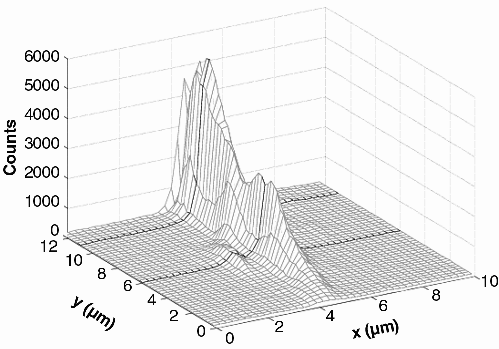
The spot size was confirmed by the resolution of a 268-times magnified image of a gold grating obtained by projection microscopy [3] where periods down to 300 nm could be clearly distinguished (Figure 164). The microanalysis device has been used for an experiment to study the wetting of a nickel bi-crystal by liquid bismuth. By scanning the sample across the X-ray focus, a microfluorescence raster image was produced. Figure 165 shows the image obtained at the bismuth L-edge with minimum feature sizes of 0.58 µm FWHM. The same KB system was further examined on the bending magnet beamline BM5 giving a spot size of 0.7 µm x 0.7 µm. We now aim at improving the stability, the mirror quality [1], and the acceptance up to 1 mm2 by using graded multilayers.
 |
Fig. 165: Bismuth L-edge microfluorescence image of a nickel bi-crystal showing 0.58 micrometres features. |
References
[1] O. Hignette, J.-C. Peffen, V. Alvaro, E. Chinchio and A. Freund, Proceedings of SPIE 4501, 43-53 (2001).
[2] O. Hignette, A.K. Freund and E. Chinchio, Proceedings of SPIE 3152, 188-199 (1997).
[3] P.Cloetens, W. Ludwig, J. Baruchel, D. van Dyck, J. van Landuyt, J.-P. Guigay and M. Schlenker, Appl. Phys. Lett. 75, 2912-2914 (1999).
Principal Publication and Authors
O. Hignette, G. Rostaing, P. Cloetens, A. Rommeveaux, W. Ludwig and A.K. Freund, Proceedings of SPIE 4499, in press.
ESRF
| <<< Previous | Contents | Next >>> |
| last modified: 4 April, 2003 by webmaster@esrf.fr | |


