- Home
- Users & Science
- Scientific Documentation
- ESRF Highlights
- ESRF Highlights 2004
- Materials Science
- Real-time Evolution of the ITO Film Properties and Structure during Annealing in Vacuum
Real-time Evolution of the ITO Film Properties and Structure during Annealing in Vacuum
Tin-doped-indium oxide In2O3:Sn (ITO) is an n-type semiconductor with high transparency and nearly metallic conductivity. Thin films of ITO find applications in optoelectronics, solar cells, and in the liquid crystal display industry. Annealing is a known way to improve the electrical and optical properties of ITO. The present investigation was performed to correlate changes of the film properties with its structural evolution during annealing in vacuum.
Amorphous 130 nm thick films were produced on Si(100) substrates covered with SiO2 by reactive pulsed magnetron sputtering using the technology described in [1]. To study the real time evolution of the film structure with experiments at the ROBL beamline (BM20), a UHV annealing chamber with an X-ray transparent beryllium dome was installed on a six-circle goniometer. The XRD data were obtained in Bragg-Brentano geometry by a multichannel position sensitive detector allowing a fast acquisition time. In experiments carried out in the ITO deposition equipment at FZR (Forschungszentrum Rossendoorf) the optical properties of the films were monitored in situ by spectroscopic ellipsometry (SE). In both experiments the annealing temperature Ta was gradually increased from 20 to 330°C with a constant rate of 5°C/min and the film resistivity was measured in situ by a four-point probe technique.
 |
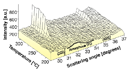
Fig. 30: Evolution of XRD patterns during annealing in vacuum. |
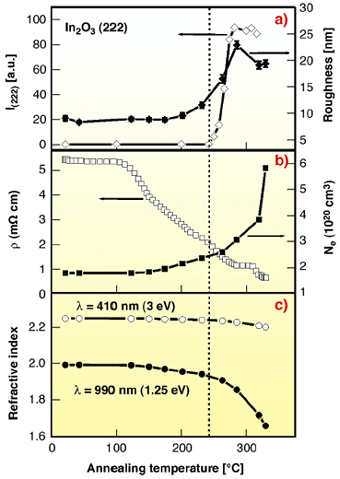
At an increase of Ta up to 250 ± 10°C, the XRD patterns show only a broad amorphous peak around 32°. The evolution of the XRD patterns within the temperature range 200-320°C is shown in Figure 30. At Ta > 250°C, the (222) and (400) peaks of crystalline In2O3 phase start to appear. Their intensity increases strongly if Ta increases by approximately 30°C, pointing to a rapid crystallisation of the film. The film becomes completely crystalline at Ta > 280°C with a stable structure above, which exhibits a weak (222) fibre texture in this state. The size of coherently diffracting domains was estimated to 65 ± 4 nm. The temperature dependence of XRD integral intensity of the In2O3 (222) peak (I(222)) (Figure 31a) shows an enhancement of the crystalline fraction during the amorphous-to-crystalline transition. Roughness growth observed by SE is correlated to the film crystallisation.
 |
Fig. 31: The temperature dependence of the XRD integral intensity of the In2O3 (222) peak (I(222)) and the film roughness (a); resistivity and free electron density Ne (b); refractive index (c). |
Using the KolmogorovJohnsonMehlAvrami equation for the time dependence of crystallisation degree f = I(222) / IC(222) = 1-exp(-Ktn), where IC(222) is the integral intensity at complete crystallisation, the kinetic exponent n = 2.99 ± 0.23 was determined. Because the coherently diffracting domain size is smaller than the film thickness, this kinetic exponent indicates a three-dimensional crystallisation process.
The temperature dependence of the resistivity in Figure 31b indicates several stages with features at Ta = 110, 150, 280 and 310°C. The behaviour of the free electron density Ne in the Figure 31b qualitatively agrees with a decrease of the resistivity, excepting the temperature range of 280-310°C. The refractive index in Figure 31c decreases at increasing annealing temperature that relates to the free electron density behaviour. The stability of the film resistivity and refractive index at a temperature below Ta ~ 120°C indicates that neither the free electron density nor the structure of the ITO films change during the first annealing period. At temperatures (120-240°C) the resistivity improvement and free electron density increase in the amorphous ITO can be attributed to the creation of oxygen vacancies due to relaxation of distorted In-O bonds in the amorphous phase.
The enhancement of the free electron density Ne after the beginning of crystallisation can be explained by the onset of Sn donor activation in a crystalline phase. However, the SE is sensitive to the free electron density enhancement even in crystalline grains, which are electrically insulated. These grains do not contribute to resistivity decrease until they are electrically connected. Maybe such connections are a reason for the drop of resistivity after a plateau observed within the temperature range 280-310°C. The comparison of the graphs in Figure 31 clearly shows that at constant heating rate the resistivity and optical properties depend non-linearly on the crystalline fraction.
In summary, the structure and properties dependency on temperature of ITO films have been monitored in real time during annealing in vacuum, using three complementary in situ techniques. The direct observation of the structure yields a crystallisation temperature of 250°C. Even in the amorphous state the film resistivity decreases significantly at increasing temperature, probably due to relaxation of distorted In-O bonds, which leads to a free electron density enhancement by the creation of oxygen vacancies. The rapid crystallisation is accompanied by film roughening and leads to a further decrease of the resistivity due to Sn donor activation.
References
[1] A.I. Rogozin, M.V. Vinnichenko, A. Kolitsch, and W. Möller, J.Vac. Sci. Technol. A22(2), 349-355 (2004).
Principal Publication and Authors
A. Rogozin (a), N. Shevchenko (a), M. Vinnichenko (b), F. Prokert (a), V. Cantelli (a, c), A. Kolitsch (a), and W. Möller (a), Appl. Phys. Lett. 85(2), 212-214 (2004).
(a) Forschungszentrum Rossendorf, Dresden (Germany)
(b) University of Kyiv (Ukraine)
(c) ROBL-CRG, ESRF


