- Home
- Users & Science
- Scientific Documentation
- ESRF Highlights
- ESRF Highlights 2007
- Materials Science
- Giant metal compression at liquid-solid (Pb-Si, In-Si) Schottky junctions
Giant metal compression at liquid-solid (Pb-Si, In-Si) Schottky junctions
Metal-semiconductor junctions -known as Schottky contacts- form the basis of the earliest man-made hybrid interface structures. The electronic structure across the Schottky contact exhibits a characteristic band deformation at the semiconductor side of the interface. It is generally accepted that no specific change in the electronic structure should be induced on the metal side of the interface, since the high-density Fermi liquid limits all electronic screening effects within the metal to a rather small interfacial layer given by the screening length in the metal, which is of the order of 1 Å.
The effect of a solid wall onto the structure of the adjacent liquid has been investigated by theory in great detail, predicting a liquid density oscillation normal to the wall with a period and decay length which are governed by the bulk nearest neighbour distance d and the bulk liquid correlation length ![]() , respectively. The experimental observation of this packing phenomenon for simple liquids is challenging and has been successful only for a very small number of systems. Here we consider liquid metals in contact with a single crystalline semiconductor surface, where we investigated the electron density profile across the interface by X-ray reflectivity.
, respectively. The experimental observation of this packing phenomenon for simple liquids is challenging and has been successful only for a very small number of systems. Here we consider liquid metals in contact with a single crystalline semiconductor surface, where we investigated the electron density profile across the interface by X-ray reflectivity.
High energy X-ray reflectivity measurements from a variety of solid-liquid Schottky interfaces have been taken at the high energy beamline ID15A using the HEMD instrument for surface and interface diffraction. The energy of the microfocused X-ray beam was typically 71 keV allowing the beam to penetrate the 20 mm long sample from the Si side of the interface at almost normal incidence. In this way only the metal-semiconductor interface is illuminated, where the incoming X-ray beam is then internally reflected. All samples have been prepared and kept in a specially designed UHV chamber during the experiments.
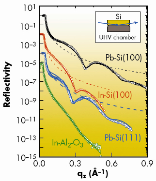
In a first experiment the X-ray reflectivity at the interface Pb(liq.)-Si(100) was measured (see Figure 25). The reflectivity exhibits pronounced oscillations pointing to the existence of density anomalies at this interface, which were found to be temperature-independent. The X-ray reflectivity could be reproduced assuming a giant densification of the liquid Pb adjacent to the interface. In order to check the conjecture that the giant densification of liquid metallic Pb in contact with Si(100) is a generic phenomenon, several control experiments were carried out, measuring X-ray reflectivity profiles from the liquid indium in contact with Si(100), liquid Pb in contact with Si(111), and liquid indium in contact with insulating Al2O3 (see Figure 25).
 |
|
Fig. 25: High energy X-ray reflectivities of different metal-semiconductor interfaces. For comparison, the reflectivity of a metal-insulator interface, In-Al2O3(001), is shown. The lines are fits using a simple two-layer model for the electron density profile across the interface. The data are shifted vertically for clarity. |
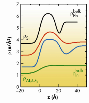
A simple two-layer model for the electron density profile across the interface was sufficient to reproduce the generic features of the reflectivity curves (lines in Figure 25). The corresponding electron density profiles are summarised in Figure 26. All metal-semiconductor interfaces are characterised by a large density increase at the interface followed by a layer with depleted density before reaching the bulk density of the liquid metal. The observation that all metal-semiconductor interfaces display similar features while the metal-insulator interface In-Al2O3(001) does not display any anomalies, suggests that charge transfer might be the origin for the interfacial density anomalies.
 |
|
Fig. 26: Electron density profiles for the interfaces Pb-Si(100), In-Si(100), Pb Si(111), and In-Al2O3(001). Oscillatory density anomalies are found only at the metal-semiconductor interfaces. The profiles are shifted by a constant offset for clarity. |
Our experiments present a new interfacial phenomenon which emerges at liquid Pb/Si and liquid In/Si interfaces. Rather straightforward high energy X-ray reflectivity measurements exhibit very unusual intensity oscillations which can only be understood assuming a giant densification of the liquid metal adjacent to the semiconductor. The densification of more than 30% points to a charge transfer phenomenon between the metal and the semiconductor leading to a shrinkage of the ionic radius of the metal ions. The thickness of this densified layer is around 1.5-2 nm and thus beyond the screening length in metals.
Principal publication and authors
H. Reichert (a), M. Denk (a), J. Okasinski (a), V. Honkimäki (b), H. Dosch (a,c), Phys. Rev. Lett. 98, 116101 (2007).
(a) Max Planck Institute for Metals Research, Stuttgart (Germany)
(b) ESRF
(c) Institut für Theoretische und Angewandte Physik, Universität Stuttgart (Germany)


