- Home
- Users & Science
- Scientific Documentation
- ESRF Highlights
- ESRF Highlights 2009
- Soft condensed matter
- Organic heterostructure growth and the role of the buried interface
Organic heterostructure growth and the role of the buried interface
The last decade has witnessed an increased emphasis on the development of devices based on organic semiconducting materials, whose attractiveness stems from their potential low production cost and the wide range of novel physical and chemical properties they offer. A key aspect for the device performance is the optimisation of the structure and morphology of the active layers, in particular in proximity to the various interfaces which play pivotal roles for the device functionality. Focusing on organic-organic heterostructures and interfaces, we report how the morphology of diindenoperylene (DIP, p-type semiconductor) films deposited on top of fluorinated cobalt-phthalocyanines (F16CoPc, n-type semiconductor) can easily be controlled by the growth temperature, ranging from smooth, layered heterostructures, to the formation of highly crystalline DIP islands.
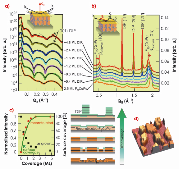
In a first step, the F16CoPc films on SiO2 were characterised by X-ray reflectivity (XRR) and grazing incidence X-ray diffraction (GIXD). Subsequently, the heterostructure growth was performed by stepwise deposition of DIP onto previously grown F16CoPc films and characterised in situ after each growth step. Figure 75 shows the XRR and GIXD data associated with a heterostructure grown at 120°C. By fitting the XRR data we access the electron density profiles of the sample, revealing, among other things, the evolution of the topmost film surface and of the organic-organic interface morphologies during heterostructure growth. The heterostructure follows a Stranski-Krastanov type of growth (i.e. wetting layer followed by island growth). Most interestingly, this growth behaviour is concomitant with a reconstruction of the two to three F16CoPc buried layers closest to the interface, as observed from the GIXD data in Figure 75b. The coincidence between the amount of reconstructed F16CoPc and the percentage of surface area covered by DIP gives insight into the reconstruction process itself, which takes place in those areas covered by the DIP wetting layer (Figure 75c). The final heterostructure features a reconstructed underlayer in proximity to the interface, a DIP wetting layer and highly crystalline DIP islands whose size and density can be tuned by coverage and growth temperature (Figure 75d). However, this is a thermally activated process, and for growth temperatures below 70°C, smooth heterostructures form and no F16CoPc reconstruction takes place at the organic-organic interface. The similarities observed with the growth of DIP on F16CuPc highlight the generality of this novel growth scenario to different fluorinated phthalocyanines [1,2].
 |
|
Fig. 75: a) XRR data (symbols) and fits (solid lines) measured in situ at different steps of the heterostructure growth at 120ºC. b) Corresponding GIXD data, highlighting the shift of the F16CoPc reflections. The insets in (a) and (b) represent the diffraction geometries. c) Normalised intensity vs. DIP coverage of the “as grown” (black squares) and reconstructed (red circles) F16CoPc (01) ßbilayer Bragg peak. The green line represents the evolution of the percentage of surface covered by DIP as obtained from the electronic density profiles fitted to the reflectivity data in (a). The schemes at the right depict the suggested growth scenario. d) AFM topography image (2x2 µm2) of a 6 ML DIP / 3 ML F16CoPc heterostructure grown at 120ºC. |
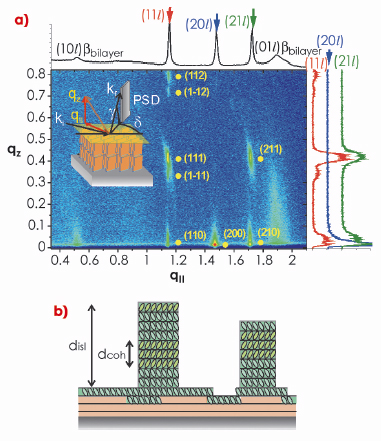
The use of a position sensitive detector (PSD) provided access to a larger portion of the reciprocal space, thereby allowing us to determine for the first time, not only the thin film structure of F16CoPc, but also the three-dimensional crystallographic structure of the DIP films/islands and their polycrystalline nature (Figure 76).
 |
|
Fig. 76: a) Two-dimensional GIXD data corresponding to 4.8 ML DIP on 2.5 ML F16CoPc grown at 120ºC. The upper spectrum corresponds to the integrated intensity along qz, while the right hand side profiles correspond to the intensity along the DIP rods. The positions for the observed DIP Bragg reflections as calculated from the optimised unit cell parameters are overlaid on the graph (shifted by 0.7 Å-1). The measurement geometry is schematically depicted in the inset. b) Schematic representation of the heterostructure, evidencing the presence of multiple coherently ordered crystalline domains within each of the islands. |
In summary, we have shown a controllable route to finely tune the morphology of organic p-n heterostructures, and have given evidence for its intimate relationship with the structure at the organic-organic interface. This study provides new insight into the mechanisms of organic heterojunction formation and their kinetics, thereby increasing the current understanding on the growth of organic materials for optoelectronic applications.
References
[1] E. Barrena, D.G. de Oteyza, S. Sellner, H. Dosch, J.O. Osso and B. Struth, Phys. Rev. Lett. 97, 076102-1-4 (2006).
[2] D.G. de Oteyza, T.N. Krauss, E. Barrena, S. Sellner, H. Dosch and J.O. Osso, Appl. Phys. Lett. 90, 243104-1-3 (2007).
Principal publication and authors
D.G. de Oteyza (a), E. Barrena (b,c), Y. Zhang (b), T.N. Krauss (b), A. Turak (b), A. Vorobiev (d) and H. Dosch (b,c), J. Phys. Chem. C 113, 4234-4239 (2009).
(a) Donostia International Physics Center, San Sebastián (Spain)
(b) Max-Planck-Institut für Metallforschung, Stuttgart (Germany)
(c) ITAP, Universität Stuttgart (Germany)
(d) ESRF


