- Home
- Users & Science
- Scientific Documentation
- ESRF Highlights
- ESRF Highlights 2013
- Structure of materials
- Perfect germanium crystals on silicon for high-resolution X-ray detectors
Perfect germanium crystals on silicon for high-resolution X-ray detectors
Highly-perfect epitaxial semiconductor layer stacks are quintessential for many low-dimensional quantum structures such as ultrafast transistors, solid state lasers and detectors. While the world’s semiconductor industry is overwhelmingly focused on silicon (Si), the first solid-state transistor was made from germanium (Ge) in 1947 [1]. Ever since then, the complexity of semiconductor technology has been increasing, driven by smaller, faster, and more cost-effective devices. For the last few decades, industry has been surprisingly successful in meeting or even surpassing the prediction of Moore’s law [2], that axiom of microprocessor development, which states that the density of transistors in integrated circuits should roughly double every two years. However, dimensional scaling following Moore’s law is approaching fundamental limits, calling for functional scaling, often described as “More-than-Moore” [3]. This involves the use of other semiconductor materials with optical and electrical properties superior to those of Si. Combining Si with other semiconductor materials raises, however, serious concerns about processing compatibilities, since in general these materials are neither lattice-matched to the Si substrate, nor are they likely to exhibit similar thermal properties. Consequently, defect formation and wafer bowing are serious obstacles.
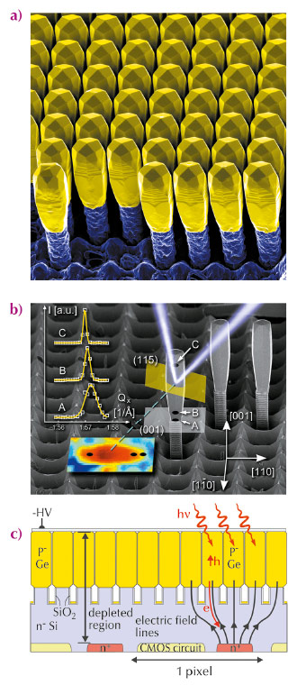
Faced with the task of producing very thick crystalline active layers made from Ge for high-efficiency and high-resolution X-ray detectors monolithically grown on Si CMOS substrates, we have shown that these problems can be solved by replacing continuous layers with arrays of closely spaced individual crystals, the fusion of which is inhibited by a new mechanism of self-limiting lateral expansion (Figure 115a) [4].
 |
|
Fig. 115: a) Colourised SEM micrograph of 8 µm tall Ge crystals grown epitaxially on Si substrates deeply patterned at the micrometre scale. b) Scanning X-ray nanodiffraction of an isolated, 11 µm tall Ge crystal. The superimposed colour map represents the scattered intensity collected around the Ge(115) peak when the incident beam was moving along the length of the crystal. The three cross-sections (yellow) of the Ge(115) peak, measured at the positions A, B and C, reveal how the Ge crystal gradually evolves into a perfect monolithic structure away from the dislocated interface. c) Concept of a high-resolution X-ray imaging detector with a monolithically integrated Ge absorber on a CMOS chip. |
The interpretation of high-resolution X-ray diffraction experiments performed with a laboratory source on such arrays was complicated by the averaging over thousands of crystals. Therefore, in order to map strain status and crystal quality locally, X-ray scanning nanodiffraction experiments were performed on individual crystals at beamline ID01 using a tightly-focused beam produced by Fresnel zone plates. To avoid signal contributions from adjacent scatterers, chosen crystals were isolated by etching and subsequent removal of their nearest neighbours. By scanning along their height, we showed that the plastic strain generated by the large mismatch of the lattice parameters between Si and Ge causes these crystals to be slightly tilted with respect to each other. Hence, the apparent mosaicity of the order of 0.1°, previously measured with laboratory sources, could be explained in terms of individual tilts of thousands of crystals. Most importantly, after reaching sufficient height, the Ge crystals become indistinguishable from perfect, defect-free single crystals (Figure 115b).
This first demonstration of perfect strain-free single crystals evolving from a heavily distorted interface with a mismatched substrate could pave the way for device applications hampered so far by dislocations, substrate bending and layer cracking. Especially the fabrication of high-brightness light-emitting diodes, radiation detectors, power transistors and multiple-junction solar cells might profit from the elimination of mismatch related defects.
As far as the ESRF’s own interests are concerned, the X-ray detection applications are probably the most interesting, because such dense arrays of perfect Ge crystals a few micrometres in width and epitaxially grown on a CMOS chip could open a route to new imaging detectors with unrivalled spatial resolution. The concept of such a detector is schematically depicted in Figure 115c. Here, the absorber layer is made from lightly p-doped Ge crystals grown on the back face of a thinned, highly resistive n-doped Si wafer. The CMOS readout circuits are fabricated on the front face of the wafer in implanted p-wells. The Ge crystals, mutually isolated electrically by an oxide passivation of the Si pillars, and the substrate together form heterojunction p-n diodes, which, under a reverse bias voltage, permit the separation of electron-hole pairs generated by X-ray photons in the Ge absorber.
Principal publication and authors
C.V. Falub (a), M. Medua (b,c), D. Chrastina (d), F. Isa (d), A. Marzegalli (e), T. Kreiliger (a), A.G. Taboada (a), G. Isella (d), L. Miglio (e), A. Dommann (f) and H. von Känel (a), Scientific Reports 3, 2276 (2013).
(a) Laboratory for Solid State Physics, ETH Zürich (Switzerland)
(b) Department of Condensed Matter Physics, Masaryk University, Brno (Czech Republic)
(c) CEITEC, Masaryk University, Brno (Czech Republic)
(d) L-NESS, Department of Physics, Politecnico di Milano, Como (Italy)
(e) L-NESS, Department of Materials Science, Università di Milano-Bicocca, Milano (Italy)
(f) Centre Suisse d’Electronique et Microtechnique, Neuchatel (Switzerland)
References
[1] W. Shockley, J. Bardeen and W.H. Brattain, Science 108, 678 (1948).
[2] G.E. Moore, Electronics 38 (8), pp. 114–117 (1965) reproduced in Proc. IEEE, 86, 82 (1998).
[3] “More-than-Moore” White Paper, W. Arden et. al. (2010); http://www.itrs.net/Links/2010ITRS/IRC-ITRS-MtM-v2 3.pdf.
[4] C.V. Falub, H. von Känel, F. Isa, R. Bergamaschini, A. Marzegalli, D. Chrastina, G. Isella, E. Müller, P. Niedermann and L. Miglio, Science 335, 1330 (2012).


