- Home
- Users & Science
- Scientific Documentation
- ESRF Highlights
- ESRF Highlights 2013
- Structure of materials
- In situ coherent X-ray diffraction reveals the surprisingly high stability of a single nano-object
In situ coherent X-ray diffraction reveals the surprisingly high stability of a single nano-object
The fascination of nanoparticles arises from both their diminutive size and the consequential size effects. They can have properties that are different from their bulk counterparts and even some characteristics that are completely new. When the dimensions are reduced, the influence of surfaces and interfaces rises disproportionately. Thermodynamics has to account for the high fraction of surface or interface atoms and reaction kinetics can be highly accelerated by fast diffusion and high reactivity at interfaces. This typically decreases the thermal stability of nano-objects. Fortunately, some nano-objects can be prepared with exceptionally perfect crystalline quality. The low defect density, steep concentration gradients and local strains can eventually decelerate diffusion and enhance the stability [1, 2]. For applications, their stability is of critical importance for functionality and reliability.
The analytical methods for studying the microstructure down to the atomic scale are constantly being improved. It is, however, still challenging to study nano-objects without averaging over non-identical objects and level inhomogeneities, and to avoid destructive sample preparation. In recent years, X-ray lens-less microscopy is gaining interest with the publication of successful studies showing an increase in spatial resolution. When the coherence length of the incident beam is larger than the diffracting object, the three-dimensional diffraction patterns can be regarded as the conversion of the object to reciprocal space. Information on the object in terms of the local density and lattice strains can be extracted. This led to the idea of adapting this method to study the interrelation between stress and diffusion.
For the experiment, an Ag/Au core-shell nanowire was chosen as a model system for several reasons: a single-crystalline structure can be prepared with virtually no growth defects and a smooth interface between Ag and Au, the interdiffusion is not complicated by the formation of intermetallics, and no oxide film forms on the surface.
Ag nanowires were grown and coated with Au inside an ultra-high-vacuum system. Single nanowires with a diameter of about 100 to 300 nm and length of several micrometres were selected and transferred to small sample-holders using ion-beam-cutting within an electron microscope. The diffraction experiment requires a large coherence length of the X-ray beam, focusing of the beam intensity on the small object, and a sensitive two-dimensional high-resolution detector, as available at beamline ID03.
 |
|
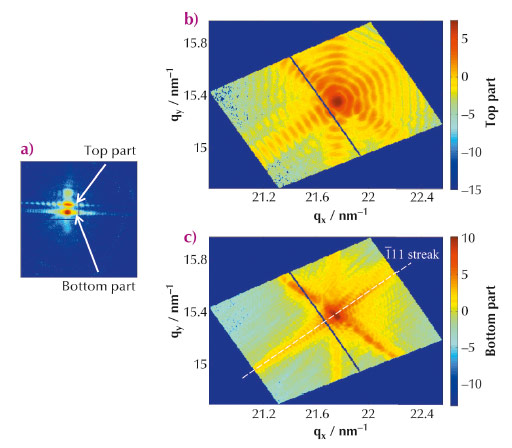
Fig. 116: Two-dimensional slices of an experimental diffraction pattern: a) parallel to the wire axis, b)-c) perpendicular to the wire axis. |
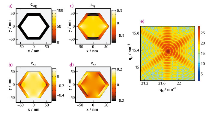
From the three-dimensional diffraction patterns, two-dimensional slices could be extracted and analysed in detail (Figure 116). Characteristic features in the diffraction patterns such as streaks, fringes and asymmetry could be directly correlated to structural features (facetted shape, size and strains) in direct space. Simulated diffraction patterns (Figure 117), considering the strain field expected from the different lattice parameters of Ag and Au, matched the experimental result well.
 |
|
Fig. 117: Simulation model of the wire cross-section: a)-d) concentration and strain field and e) calculated diffraction pattern. |
This nanowire was then subjected to in situ annealing. Even after annealing for more than one hour at 400°C, a core-shell morphology was preserved. From bulk, single-crystal diffusion data, much faster intermixing was expected for these temperatures.
This coherent diffraction experiment at beamline ID03 proved the feasibility of such an in situ diffusion study and it also revealed an increased stability of a nano-object due to its low defect-density.
For future experiments, further advancements of the experimental conditions together with improved phase-retrieval algorithms should allow the inversion of three-dimensional diffracted intensity for different beam energies. The strain and concentration fields could then be evaluated “directly”, which should unveil more surprises from the nano-world.
Principal publication and authors
S.T. Haag (a,b), M.-I. Richard (b,c), U. Welzel (a), V. Favre-Nicolin (d,e), O. Balmes (c), G. Richter (a), E.J. Mittemeijer (a,f) and O. Thomas (b), Nano Lett. 13, 1883–1889 (2013).
(a) Max Planck Institute for Intelligent Systems, Stuttgart (Germany)
(b) Aix-Marseille Université, CNRS, IM2NP UMR 7334, Marseille (France)
(c) ESRF
(d) CEA-UJF, INAC, SP2M, Grenoble (France)
(e) Université Grenoble-Alpes, Grenoble (France)
(f) Institute for Materials Science, University of Stuttgart (Germany)
References
[1] Z. Erdelyi and D.L. Beke, J. Mater. Sci. 46, 6465 (2011).
[2] J. Svoboda and F.D. Fischer, Acta Mater. 59, 1212 (2011).


