- Home
- Users & Science
- Scientific Documentation
- ESRF Highlights
- ESRF Highlights 2013
- Structure of materials
- Local structure of organic photovoltaic devices by combined X-ray diffraction and fluorescence investigation
Local structure of organic photovoltaic devices by combined X-ray diffraction and fluorescence investigation
In the continuous quest for inexpensive, low-environmental impact, renewable energy sources, the advent of polymer-based organic photovoltaic (OPV) devices has paved the way for the introduction of cheap and efficient methods to produce energy from light conversion into electricity.
Nowadays, polymer-based materials are ubiquitous in almost every aspect of modern society, as they display important advantages such as simple chemical processing and inexpensive fabrication of thin films via vacuum evaporation or solution casting technologies.
Tremendous progress in OPV devices has been achieved with the introduction of bulk heterojunction (BHJ) solar cells based on donor-acceptor blends, typically a conjugated polymer and a soluble fullerene derivative [1-3]. However, device efficiency has not yet reached the level of maturity needed to cope with the stringent requirements of routine industrial production. Novel solutions must therefore be found to harvest light in a more efficient way. A promising approach is the use of metallic nanoparticles, which strongly absorb light in the UV–visible region. This feature is attributed to both light scattering and localised surface plasmon resonance (LSPR) effects. In this respect, plasmonic nanoparticle-based OPV devices could herald a technological revolution towards high performance and durable solar cells [2,3].
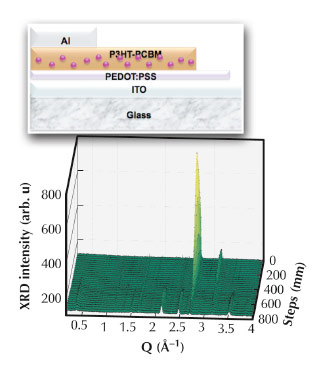
An unprecedented experiment combining X-ray diffraction (XRD) and fluorescence (XRF) with nanometre resolution on post-fabricated OPV devices doped with Au nanoparticles was performed at beamline ID11. By scanning the OPV cross-section with a ~ 100 nm focused X-ray beam, the structural properties of the different layers and interfaces comprising the device as well as the nanoparticle distribution were investigated in situ.
 |
|
Fig. 118: Schematic representation of the OPV cell studied and waterfall diagrams of XRD patterns collected during a vertical scan of the device. |
The layout of the OPV cell used for the experiment is shown in Figure 118. During the measurements, the device was translated vertically from the Al top electrode to the ITO layer, while the XRD patterns were continuously recorded (Figure 118). As the beam size was comparable to the thickness of the different layers, the scanning procedure allowed us to discriminate the diffraction signals from the individual layers.
The measurements provided an accurate space-resolved description of the molecular ordering of the polymer component of the photo-active layer. Such information is crucial, since the photovoltaic energy conversion rate strongly depends on the nanoscale phase separation during the donor/acceptor heterojunction formation as well as the nanomorphology of the interfaces formed between the active and the charge-collecting layer.
The accuracy of the experimental technique also made it possible to measure the nanoparticle distribution profile across the device thickness.
Thermal annealing performed in situ allowed the chemical-physical phenomena to be uncovered. This modification of the local nanostructure and organisation, interface effects and interdiffusion processes occur as a consequence of the annealing process that is applied to optimise organic solar cell efficiency. The results are in agreement with the significant improvement of the photovoltaic performance for the annealed devices as compared to that of pristine devices: the PV efficiency (calculated from the measured current–voltage characteristics under a solar simulator) was almost quadrupled.
The simultaneous XRF measurements are consistent with XRD findings and corroborate them. The fluorescence line intensities are shown in Figure 119 versus the vertical scanning step for each metallic element in the OPV.
 |
|
Fig. 119: In situ spatially-resolved X-ray study of an integrated organic photovoltaic device: fluorescence line intensities versus vertical scanning. |
These results represent a big step towards the elucidation of the structure-property relationships that link different length scales, from local nano/hetero structures and interfaces to large-scale devices. As such, they may be considered as a milestone in a better understanding of how the performance of OPV cells is correlated to the morphology of their respective components on the nanoscale, an essential step towards new strategies for the development of highly efficient devices.
Principal publication and authors
B. Paci (a), D. Bailo (a), V. Rossi Albertini (a), J. Wright (b), C. Ferrero (b), G.D. Spyropoulos (c,d), E. Stratakis (d) and E. Kymakis (c), Advanced Materials 25, 4760–476 (2013).
(a) Istituto di Struttura della Materia, C.N.R., Rome (Italy)
(b) ESRF
(c) Technological Educational Institute of Crete, Heraklion (Greece)
(d) Foundation for Research and Technology-Hellas and University of Crete, Heraklion (Greece)
References
[1] A.C. Mayer, S.R. Scully, B.E. Hardin, M.W. Rowell and M.D. Mc Gehee, Mater. Today 10, 11, 28 (2007).
[2] B. Paci, A. Generosi, V.R. Albertini, G.D. Spyropoulos, E. Stratakis and E. Kymakis, Nanoscale 4, 7452 (2012).
[3] B. Paci, G.D. Spyropoulos, A. Generosi, D. Bailo, V.R. Albertini, E. Stratakis and E. Kymakis, Adv. Funct. Mater. 21, 3573 (2011).


