- Home
- Users & Science
- Scientific Documentation
- ESRF Highlights
- ESRF Highlights 2014
- Soft condensed matter
- Crystal structure of conjugated polymers: a combined scattering and atomistic simulation approach
Crystal structure of conjugated polymers: a combined scattering and atomistic simulation approach
Organic photovoltaics (OPV) is a promising technology with the potential to deliver a cheap, lightweight, flexible and large area solution for niche applications in electricity generation. In polymer OPV devices, light is harvested by a low-bandgap conjugated polymer with an absorption band closely matching the solar spectrum. Upon photo-excitation of the polymer, a coulombically bound electron-hole pair, called an exciton, is formed. Exciton dissociation into free charge carriers occurs when a second material with higher electron affinity, typically a fullerene derivative, is blended with the polymer to form the so-called bulk-heterojunction. This blend can be solution processed, leading to thin films around 100 nm, and subsequently sandwiched between two electrodes with different work functions to complete the device.
Device performance is strongly affected by the microstructure of the polymer-fullerene blends, which in turn is influenced by the processing conditions and the chemical structure of the blend components. For instance, the nature of the side chains attached to the conjugated backbones to solubilise the polymer and side chain attachment can strongly influence polymer packing, and thus influence both the polymer crystallisation and the polymer:fullerene phase separation.
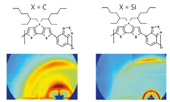
We studied a number of cyclopentadithiophene-co-benzothia-diazole polymer derivatives differing in the heteroatom (carbon or silicon, see Figure 41) that links the side chains to the cyclopentadithiophene unit and in the structure of the side chains (2-ethylhexyl, 3,7-dimethyloctyl and hexadecyl). Previous studies had shown that the photocurrent produced by a solar cell could be greatly increased by substituting the carbon heteroatom with a silicon atom or by processing the carbon analogue with additives. This effect had been assigned to a higher tendency of the silicon-substituted polymer to crystallise leading to more pronounced phase separation in the blend.
 |
|
Fig. 41: GIWAXS 2D diffraction pattern of a) poly[2,1,3-benzothiadiazole-4,7-diyl-[4,4-bis(2-ethylhexyl)-4H-cyclopenta[2, 1-b:3,4-b’]-dithiophene-2,6-diyl]] (C-PCPDTBT) and b) poly(4,4-dioctyldithieno(3,2-b:2’,3’-d)silole-2,6-diyl-alt-(2,1,3-benzo-thiadiazole)-4,7-diyl) (Si-PCPDTBT). Adapted with permission from A.A.Y. Guilbert et al., Chemistry of Materials 26, 1226-1233 (2014). Copyright (2014) American Chemical Society. |
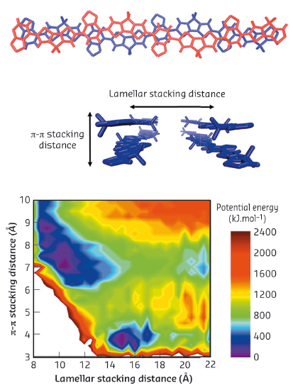
Grazing-incidence wide-angle X-ray scattering (GIWAXS) offers us the possibility to investigate the crystalline structure of such conjugated polymer in thin films. Figure 41 displays the GIWAXS pattern for the carbon and silicon analogue taken with a MAR SX-165 area detector at BM28 – the XMaS beamline. The silicon analogue, which displays a better defined diffraction pattern, shows a higher tendency to crystallise than the carbon analogue. From the patterns, we notice that the crystals of the two analogues are oriented differently with respect to the substrate. By substituting the carbon atom with a silicon atom, the π−π stacking distance (the distance between the flat, conjugated backbones of the polymers when stacked on top of one another cofacially) decreases at the cost of increasing the lamellar stacking distance (the lateral distance between polymer backbones, arranged in a sheet). This is illustrated in Figure 42.
 |
|
Fig. 42: Structure used for potential energy surface calculations showing the π−π stack and the lamellar stack. Calculated potential energy surface (PES) for C-PCPDTBT. The step size is 0.25 Å for the π−π stacking and 0.5 Å for the lamellar stacking. The PES is not shown for Si-PCPDTBT since no noticeable differences can be observed. Adapted with permission from A.A.Y. Guilbert et al., Chemistry of Materials 26, 1226-1233 (2014). Copyright (2014) American Chemical Society. |
To bridge the gap between chemical structure and crystal structure, we combine GIWAXS with molecular dynamics simulations (MD). From the quantum chemical calculations, it appears that cis and trans conformations between the cyclopentadithiophene and benzothiadiazole units are more likely and that the side chains of the silicon analogue are more flexible. We built a crystal structure with polymers in the trans configurations, a π−π stack featuring a two-fold axis parallel to the main chain axis simply translated to create the lamellar stack (See Figure 42). Then, we scanned the energy surface of this structure while varying the π−π stacking and lamellar stacking distances (for each configuration, the side chains are relaxed by performing a MD simulation at 300 K in a NPT ensemble, see Figure 42). No difference can be observed for the carbon and silicon, but both display two minima. The π−π stacking and lamellar stacking distances of one of the minima agrees very well with the distances extracted from the GIWAXS pattern of the silicon analogue. The other minimum displays a lamellar stacking in agreement with the carbon analogue but the π−π stacking is overestimated. In further studies of structures with longer and less bulky side chains, we found only one minimum corresponding to the short π−π stacking distance and long lamellar distance and in good agreement with previous reports.
We propose that the greater side chain flexibility of the silicon bridged polymer enables that material to find the minimum with the shorter π−π stacking distance, which should enable improved hole transport, leading to the higher hole mobilities that have been observed and to easier photocurrent generation in a solar cell. These studies confirm that structural characterisation using GIWAXS combined with molecular modelling can help to explain difference in performance of organic electronic materials in terms of their chemical structure and packing tendency.
Principal publication and authors
A.A.Y. Guilbert (a), J.M. Frost (a), T. Agostinelli (a,b), E. Pires (c), S. Lilliu (c,d), J.E. Macdonald (c) and J. Nelson (a), Chemistry of Materials 26, 1226-1233 (2014).
(a) Centre for Plastic Electronics, Department of Physics, Blackett Laboratory, Imperial College London (UK)
(b) Plastic Logic Ltd., Cambridge (UK)
(c) School of Physics and Astronomy, Cardiff University (UK)
(d) Masdar Institute of Science and Technology, Abu Dhabi (United Arab Emirates)


