- Home
- Users & Science
- Scientific Documentation
- ESRF Highlights
- ESRF Highlights 2016
- Structure of materials
- Real-time X-ray imaging of silicon wafer fracture
Real-time X-ray imaging of silicon wafer fracture
Fracture and breakage of single crystal silicon wafers is a severe problem for the semiconductor industry leading to million dollar costs. It is a fast and multi-lengthscale process. Crack propagation has been observed for the first time in situ simultaneously by direct transmission and diffraction X-ray imaging. The movies reveal the dynamics of strain and provide visualisation of the crack tip with a time resolution of µs/frame.
Wafer breakage during high temperature processing is a severe problem in semiconductor device manufacturing. Silicon wafers typically contain microcracks resulting from handling or shipping. Catastrophic total wafer breakage may result from such microcracks during thermal processing in semiconductor manufacturing and it is an increasingly expensive hazard for production [1]. The direct observation of cracks is a challenge because cracks can propagate in silicon with speeds of up to 1500 m/s and 3500 m/s along {110} and {111} cleavage planes respectively. Especially irregular fracturing may result in catastrophic wafer shattering, producing many small irregular pieces instead of cleaving into two pieces with smooth {110} faces.
Unprecedented temporal resolution with X-ray imaging can be reached at synchrotron light sources thanks to high-speed cameras and polychromatic illumination [2]. Recently, mechanically induced cracks in glass could be depicted by “single-bunch imaging” with exposure times short enough to exploit the pulsed time-structure of the ESRF X-ray source. We have now combined direct transmission imaging with Laue topography at beamline ID19 to successfully track crack propagation in silicon wafers: an indirect detector acquired images in radiographic mode of the crack propagation by means of phase contrast and an intensifier-based detector coupled via a lens-system to a CMOS camera recorded images of the 220 reflexion from the same event (both detectors used a 1.28 µs exposure time, ca. 35,500 images/s frame rate limited only by the camera).
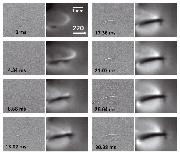
To create reproducible starting conditions for the cracks, standard (001) silicon wafers were damaged artificially using the nano-indentation technique. Subsequently, to induce thermal stresses and initiate cracking from an indent, the silicon wafer was heated up to about 1000°C by a gas burner and then quenched with a water jet while the movies were acquired. The increase of strain fields in a hot silicon wafer induced by water was resolved from the moment before new cracks nucleate until propagation stops. Figure 63 shows selected direct transmission and diffraction images of a relatively slow-growing crack. The first segment nucleates at the indent which is outside the region of interest. The inclined part deflects into the horizontal part which runs, at the front surface of the wafer, perfectly parallel to crystal plane [1-10]. With an acquisition rate of 35,511 images/s, the temporal spacing between two frames was 28.1 μs. The first image shown was taken after the first water droplets hit the hot wafer, i.e. thermal stress is already present. Single water droplets as well as water wavefronts are visible in the direct transmission images.
 |
|
Fig. 63: Selected images from a series of 3000 showing crack propagation in a silicon wafer under thermal stress. In each pair of images, the direct transmission image is on the left and the diffraction image with the 220 reflection is on the right. |
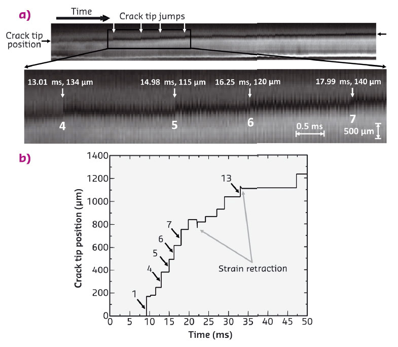
Further details about the dynamics of the propagation of crack are revealed when looking at intensity profiles: the position of the crack tip is accessible indirectly, i.e. by the local change of the grey-level intensity of the strain related contrast while the tip propagates. In Figure 64 these profiles are plotted as a function of time for the movie related to the pictures shown in Figure 63, starting with the frame where the first indication of a crack appears. The position of the crack tip is associated with the marked black region. Two features are visible immediately: (i) high-frequency oscillations due to vibrations of the wafer related to the impinging water and (ii) strong discontinuities (4 out of 13 are marked with white arrows). The latter clearly indicate that the crack does not propagate with constant velocity. Hence, the mean slow propagation speed observed (of about 0.055 m/s) results from pinning and reinitiating of the fast propagation of the crack tip.
 |
|
Fig. 64: a) Propagation of the crack tip as derived from the intensity profiles for all frames of the movie related to Figure 63. The position of the crack tip can be tracked indirectly as the tip changes the grey levels locally while travelling. The magnified region shows that the crack propagates in jumps. b) A plot of the crack tip position vs time. |
Real-time imaging with two high speed detector systems is a big step towards "truly real-time" imaging and the in situ study of processes in the 100-picosecond range. Studying cleavage and fracture in single crystals becomes possible in a combined direct visualisation and diffraction mode and the power of such high speed imaging has been demonstrated by the example of silicon wafer fracture.
Principal publication and authors
Real-time direct and diffraction X-ray imaging of irregular silicon wafer breakage, A. Rack (a), M. Scheel (b) and A.N. Danilewsky (c), IUCrJ 3, 108-114 (2016); doi: 10.1107/S205225251502271X.
(a) ESRF
(b) Synchrotron Soleil, Gif sur Yvette (France)
(c) Crystallography, Albert-Ludwigs Universität Freiburg (Germany)
References
[1] B.K. Tanner et al., International Journal of Fracture 195, 79 (2015).
[2] A. Rack et al., Journal of X-ray Science and Technology 18, 429 (2010).


