- Home
- News
- Spotlight on Science
- Perfect crystals...
Perfect crystals evolving from highly-mismatched epitaxial structures
05-11-2013
Highly-perfect epitaxial semiconductor layer stacks are quintessential for many low-dimensional quantum structures such as ultrafast transistors, solid state lasers and detectors. When semiconductor materials significantly differ in lattice parameters and thermal properties, it becomes an impossible task to keep the epitaxial structures defect-free, especially for those device applications in which layer thicknesses of many micrometres is a must, such as high-brightness light-emitting diodes, radiation detectors, power transistors and multiple-junction solar cells. However, research at beamline ID01 has demonstrated that highly mismatched layer-substrate systems, such as germanium on silicon, evolve into perfect monolithic heterostructures when the substrate is deeply patterned at the micrometre scale. Replacing continuous layers by quasi-continuous crystal arrays may thus be the key for device applications that have been hampered so far by dislocations, substrate bending and layer cracking.
Share
Ever since the invention of the transistor in 1947, the complexity of semiconductor technology has been increasing, driven by faster, more cost-effective devices. For the last few decades, industry has been surprisingly successful in meeting the prediction of Moore’s law [1], that axiom of microprocessor development, which states that the density of transistors in integrated circuits should roughly double every two years.
However, dimensional scaling following Moore’s law is approaching fundamental limits, calling for functional scaling, often described as “More than Moore” [2]. This involves the use of other semiconductor materials with optical and electrical properties superior to those of silicon. For example, devices such as high-brightness light emitting diodes, power transistors, and radiation detectors monolithically grown on large Si wafers, if feasible, could enhance functionality and greatly lower manufacturing and materials costs. Combining Si with other semiconductor materials raises, however, serious concerns about materials and processing compatibilities, since in general these materials are neither lattice-matched to the Si substrate, nor are they likely to exhibit similar thermal properties. Consequently, wafer bowing and defect formation are serious obstacles.
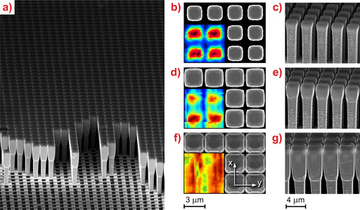
Faced with the problem of producing very thick crystalline active layers made from germanium (Ge) for high-efficiency and high-resolution X-ray detectors, monolithically grown on Si CMOS substrates, we have shown that these problems can be solved by replacing continuous layers with arrays of closely spaced individual crystals, the fusion of which is inhibited by a new mechanism of self-limiting lateral expansion (Figure 1a) [3].
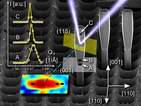
High-resolution X-ray diffraction experiments performed with a laboratory source on such arrays were obscured by averaging over thousands of crystals because of the large size of the X-ray beam. Therefore, in order to map strain status and crystal quality locally, X-ray scanning nanodiffraction experiments were performed at the ID01 beamline. By scanning individual crystals with an 11.07 keV X-ray beam focused down to ~300 × 500 nm using Fresnel zone plates (FZP), we revealed how misfit and thermal strains of these high-aspect ratio structures evolve.
First of all, for relatively short Ge crystals with heights of a few micrometres, for which the mixed signals from adjacent crystals can still be separated (Figure 1b-e), we showed how elastic relaxation of the thermal strain formed during cooling from the growth temperature leads to diminishing lattice bending as the crystals gain in height. However, taller crystals could not be localised within the array due to the shallow incidence angle, ~46° for the (115) Bragg reflection (Figure 1f,g). Therefore, isolated crystals were prepared by etching and subsequent removal of the neighbouring crystals using micromanipulators inside a scanning electron microscope. By scanning these crystals along their heights, we showed that the plastic strain generated by the large mismatch of the lattice parameters between Si and Ge (~4.2 %) causes these crystals to be slightly tilted with respect to each other, as an effect of the distinctive misfit dislocation networks of the crystals. Hence, the apparent mosaicity of the order of 0.1°, previously measured with laboratory sources, could be explained as individual tilts of thousands of crystals. Most importantly, after reaching sufficient height, the Ge crystals become indistinguishable from perfect, defect-free single crystals (Figure 2). This is in fact the first demonstration of perfect strain-free single crystals evolving from a heavily distorted interface with a mismatched substrate.
Using existing state-of-the-art methods, electrical contacts could be made to the individual Ge crystals, a few micrometres in width and epitaxially grown on a CMOS chip. This would open a route to X-ray imaging detectors with enormous spatial resolution. Moreover, the concept of substrate patterning and epitaxial growth can be extended to other material combinations in the areas of high-efficiency solar cells and power electronic devices.
Principal publication and authors
Perfect crystals grown from imperfect interfaces, C.V. Falub (a), M. Meduňa (b,c), D. Chrastina (d), F. Isa (d), A. Marzegalli (e), T. Kreiliger (a), A.G. Taboada (a), G. Isella (d), L. Miglio (e), A. Dommann (f), and H. von Känel (a), Scientific Reports 3, 2276 (2013).
(a) Laboratory for Solid State Physics, ETH Zürich (Switzerland)
(b) Department of Condensed Matter Physics, Masaryk University, Brno (Czech Republic)
(c) CEITEC, Masaryk University, Brno (Czech Republic)
(d) L-NESS, Department of Physics, Politecnico di Milano, Como (Italy)
(e) L-NESS, Department of Materials Science, Università di Milano-Bicocca, Milano (Italy)
(f) Centre Suisse d’Electronique et Microtechnique, Neuchatel (Switzerland)
References
[1] G.E. Moore, Electronics 38 (8), pp. 114–117 (1965) reproduced in Proc. IEEE, 86, 82 (1998).
[2] “More-than-Moore” White Paper, W. Arden et. al. (2010); http://www.itrs.net/Links/2010ITRS/IRC-ITRS-MtM-v2 3.pdf
[3] C.V. Falub, H. von Känel, F. Isa, R. Bergamaschini, A. Marzegalli, D. Chrastina, G. Isella, E. Müller, P. Niedermann, L. Miglio, Science 335, 1330 (2012).
Top image: Germanium crystals grown epitaxially on deeply patterned silicon substrates.


