- Home
- Users & Science
- Scientific Documentation
- ESRF Highlights
- ESRF Highlights 2002
- Materials Science
- Fundamental Studies in Materials Science: Microstructure Development in 3D
Fundamental Studies in Materials Science: Microstructure Development in 3D
A longstanding problem in materials research is the lack of any robust quantitative modelling to predict a material's microstructure after processing. For example this may consist of mechanical deformation, heat treatments, and other often complex processing steps that have been developed by years of educated trial and error. The relationship between microstructure and physical properties is better understood. For example, the strength, ductility, and electromagnetic properties of materials are strongly dependent on the microstructure such as grain size, grain boundary morphology, and orientation distribution of grains (texture). For this reason, a more fundamental understanding of the development of microstructure during thermo-mechanical processing is of great importance in order to facilitate the development of future generations of engineering materials.
New developments in the understanding and modelling of microstructure evolution have, in general, followed directly from the emergence of new experimental techniques. New developments in optical microscopy led to the first confirmation of slip along preferred crystallographic planes as a mechanism for plastic deformation. Further developments came with the availability of electron microscopy. For the first time microstructure could be observed from the grain to the dislocation level. The result of these new experimental techniques was an explosion of theoretical work on the dynamics of dislocation motion and the kinetics of grain nucleation and growth. Although these techniques have brought materials science from a black art to a true scientific discipline, a number of problems are still associated with the currently available characterisation techniques, which have prevented the next breakthrough in microstructural development modelling. The major disadvantage of the traditional microscopy methods (optical, SEM, TEM, etc.) is that they are primarily surface measurements unable to probe microstructure deeply embedded within bulk materials. It is well known that the surfaces of materials are non-representative of the bulk due to stress relaxation at the surface and dislocation migration. Serial sectioning can provide 3D data but being a destructive technique does not allow direct studies on the dynamics.
What is needed then is a technique that is able to provide non-destructive 3D information on the microstructure of materials. The penetrating power of high energy X-rays (> 50 keV) allows for bulk sampling (from mm to cm depending on the material). This has been routinely used for bulk strain and texture measurements at neutron and synchrotron facilities. These techniques, though, rely on powder diffraction methods, and therefore give only average information of ensembles of grains. More advanced models need a finer microstructural map as they incorporate interactions between neighbouring grains. Powder average measurements are unable to address such issues.
The second hutch of ID11, the materials science beamline, has been built as a dedicated instrument for the development of techniques for measuring the microstructure of individual grains (and sub grains in certain cases) within bulk 3D volumes. In general, we refer to this instrument as the three-dimensional X-ray diffraction (3DXRD) microscope. Currently a number of techniques have been developed which allow for measurements of grain morphology (a 3D equivalent of an SEM micrograph), individual grain orientations, strain tensors of individual grains, and structural refinement of individual grains. About 100-1000 grains can be measured simultaneously, either statically or as a function of applied stress or temperature. Increasing statistics at the individual grain level have already invalidated a number of traditional models. Further statistics should allow us to reach the proper constraints necessary for the next generation of models.
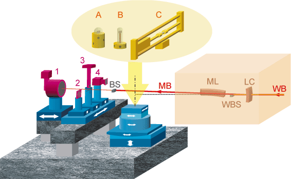
The basic design of the 3DXRD is shown in Figure 76. The optics consists of a bent Laue crystal, which acts as a monochromator and vertical focusing element, and a bent multilayer, which focuses horizontally. This provides a minimum spot size of 2 x 5 µm at energies between 50 and 90 keV.
 |
|
Fig. 76: Optics: WB: White beam; LC: Bent Laue crystal; ML: Bent multilayer; WBS: White beam stop; MB: 2-dimensionally micro-focussed monochromatic beam; BS: Monochromatic beam stop. Sample environment (yellow): A: Cryostat; B: Furnace; C: 25 kN stress rig. Detectors / slits (purple): 1: Large area detector; 2: Conical slit system; 3: High-resolution area detector; 4: Optional detector. |
The sample stage provides for x-y-z translations with a 1 µm precision and a rotation table with a sphere of confusion of less than 1 µm. The sample stage has been designed to allow for a wide variety of sample environments including furnaces, cryostats, and stress rigs. Finally we have a number of detector systems, which may be translated in order to allow for a variety of measurements on the same sample. A brief description of the major techniques will be given with a short example of experimental results.
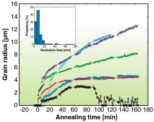
The most basic detector configuration of the 3DXRD utilises a large area detector (FRELON coupled to an image intensifier). In this configuration the full thickness of the sample is probed. If the illuminated volume contains up to several hundreds of grains then each individual grain can be indexed simultaneously as to its orientation and volume. The indexing is automated by software developed specifically for the instrument [1]. In order to define a gauge volume within the sample, a conical slit cell may be inserted between the sample and detector. This cell has 7 conically-shaped openings of 20 µm (corresponding to cubic reflections). With the conical slit in place, a 250-300 µm gauge length is defined along the beam direction [2]. The focal point of the conical slit then acts as a fixed position in 3D space with which to locate grains positions. This system is ideal for measuring the kinetics during thermo-mechanical processing. A tensile stress rig can be mounted on the sample stage and the orientation of individual grains can be measured as a function of applied load. The rotation pathway of individual grains can then be compared directly to texture models, which previously had only been tested by measurements on ensembles of grains (which inherently assumes no grain-grain interactions). Current results on 100 grains show significant deviations from classical models [3]. The kinetics of nucleation and grain growth may also be examined on the level of individual grains for the first time. By mounting a furnace on the sample stage the nucleation and growth of grains can be monitored in situ. Figure 77 shows growth curves for a number of grains [4]. Again the results are in disagreement with classical models (Avrami). In particular, growth rates can vary by an order of magnitude and individual grains may have varying incubation time. Statistics on the order of 1000 grains have been measured to date and correlations between growth rate and orientation are being used to modify existing models. Similar measurements have been recently done on the kinetics of phase transformations of steels and further information is given in a later highlight (Offerman et al.).
 |
|
Fig. 77: Growth curves for 6 random grains are shown to illustrate the large spread in growth kinetics. The inset shows the distribution of nucleation times given a threshold of 1.3 µm. |
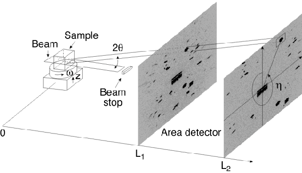
A high-resolution camera (5 µm point spread) is also mounted on the detector arm. This camera is used to create 3D grain maps with a spatial resolution limited by the resolution of the camera. The technique is in essence a virtual 3D detector. In this case only vertical focusing is used so that a single layer is illuminated. The detector is placed close to the sample (5 mm) so that the shape of the diffraction spots are projections of the grains shape and not dominated by divergence. The detector is then translated along the beam direction in order to track each reflection back to the sample plane [5] (Figure 78). Translating the sample height then allows a full 3D map of the grain boundaries and grain orientations to be reconstructed.
 |
|
Fig. 78: Illustration of the tracking technique. When the detector is translated away from the sample the diffraction spots will move outwards on the detector. The positions of the diffracting grains in the sample are determined by linear fits. The fits also provide the 2 |
By combining the various techniques outlined above it is possible to follow the microstructural development by measuring the boundary morphology, size, orientation, and elastic strain tensor of each grain within the volume of interest during thermo-mechanical processing. As the spatial resolution is tunable, it is also possible to zoom out in order to perform materials engineering studies of the local stress and texture. Although the examples given here have focused on thermo-mechanical processing of metals it should be emphasised that this is a general technique which has already been applied to a variety of problems including high temperature superconductor processing, texture development in polymers, and a large variety of phase transformations. With the introduction of the 3DXRD technique it is hoped that theoretical development will follow suit and a better understanding of the fundamental processes which govern microstructure development will lead not only to a firmer understanding of basic materials science but also lead to a new generation of materials with improved physical properties.
References
[1] E.M. Lauridsen, S. Schmidt, R.M. Suter and H.F. Poulsen, J. Appl. Cryst. 34, 744-750 (2001).
[2] S.F. Nielsen, A. Wolf, H.F. Poulsen, M. Ohler, U. Lienert, and R.A. Owen, J. Synch. Rad., 7, 103-109 (2000).
[3] L. Margulies, G. Winther and H.F. Poulsen, Science 291, 2392-2394 (2001).
[4] E.M. Lauridsen, D.J. Jensen, H.F. Poulsen and U. Lienert, Scripta matter 43, 561-566 (2000).
[5] S.F. Nielsen, W. Ludwig, D. Bellet, E.M. Lauridsen, H.F. Poulsen and D.J. Jensen, (Eds) N. Hansen, X. Huang, D.J. Jensen, E.M. Lauridsen, T. Leffers, W. Pantleon, T.J. Sabin and J.A. Wert, Proc. of 21st Risø International Symposium on Materials Science, Risø 4-8 September, 473-478 (2000).
Authors
L. Margulies (a,b), D.J. Jensen (a), E.M. Lauridsen (a), R.V. Martins (a), S.F. Nielsen (a), H.F. Poulsen (a) and S. Schmidt (a).
(a) Risø National Laboratory, Roskilde (Denmark)
(b) Risø Scientist in Residence at the ESRF
 and
and  values for grain indexing.


