- Home
- Users & Science
- Scientific Documentation
- ESRF Highlights
- ESRF Highlights 2005
- High Resolution and Resonance Scattering
- Hard X-ray Photoemission Spectroscopy from Solids with High Energy Resolution and Bulk Sensitivity
Hard X-ray Photoemission Spectroscopy from Solids with High Energy Resolution and Bulk Sensitivity
Photoemission spectroscopy (PES) is a powerful tool to investigate the electronic properties of materials, with impressive technical achievements in terms of energy, momentum, and angular resolution. Over the last two decades, PES experiments with synchrotron radiation exploited one of the key features of this technique, i.e. its surface sensitivity. By tuning the kinetic energy Ek of photoelectrons to the minimum of their mean free path ![]() in the solid, the measurement is sensitive to the topmost atomic layers only. However, this poses severe limitations to the investigation of bulk electronic properties. The use of hard X-rays (5-10 keV) is a possible route to perform volume sensitive PES. After the pioneering experiment by Lindau et al. [1], the development of Hard X-ray PES (HAXPES) has been restrained mainly by the poor resolving power of both photon source and electron analyser. Technical conditions have since improved considerably on modern high-resolution/high-flux beamlines, giving new impetus to the measurement of bulk sensitive PES spectra [2].
in the solid, the measurement is sensitive to the topmost atomic layers only. However, this poses severe limitations to the investigation of bulk electronic properties. The use of hard X-rays (5-10 keV) is a possible route to perform volume sensitive PES. After the pioneering experiment by Lindau et al. [1], the development of Hard X-ray PES (HAXPES) has been restrained mainly by the poor resolving power of both photon source and electron analyser. Technical conditions have since improved considerably on modern high-resolution/high-flux beamlines, giving new impetus to the measurement of bulk sensitive PES spectra [2].
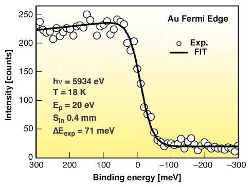
We have developed a new electron spectrometer (VOLPE: VOLume PhotoEmission from solids) dedicated to HAXPES experiments and now fully operational at beamline ID16. During the commissioning phase, we tested the performance of our spectrometer in terms of energy resolution and probing depth, using polycrystalline noble metals and wedge-shaped thin layers grown on Silicon substrates, respectively. Figure 12 shows the Fermi level of polycrystalline Au measured at T = 18 K and h![]() = 5934 eV. The total width of the Fermi edge is given by the temperature broadened Fermi distribution, convoluted with a Gaussian whose FWHM equals the overall experimental resolution (electron analyser + photons). The best fit (solid line in Figure 12) was obtained using a FWHM of 71 ± 7 meV, corresponding to a resolving power of 8x10⁴. The photon energy resolution was measured independently to be 50 meV, giving, for the analyser alone, an energy resolution of 51±8 meV (resolving power of 1.2 x 10⁵).
= 5934 eV. The total width of the Fermi edge is given by the temperature broadened Fermi distribution, convoluted with a Gaussian whose FWHM equals the overall experimental resolution (electron analyser + photons). The best fit (solid line in Figure 12) was obtained using a FWHM of 71 ± 7 meV, corresponding to a resolving power of 8x10⁴. The photon energy resolution was measured independently to be 50 meV, giving, for the analyser alone, an energy resolution of 51±8 meV (resolving power of 1.2 x 10⁵).
 |
|
Fig. 12: Au Fermi level (circles) measured at hv = 5934 eV with pass energy Ep = 20 eV and analyser slits sin = 0.4 mm. The acquisition time was 150 minutes and the counts correspond to an integration over 8 mm of detector active area. The overall energy resolution, as obtained from the fit of the Fermi edge (solid line), is about 71 meV FWHM (50 meV photons + 50 meV analyser). |
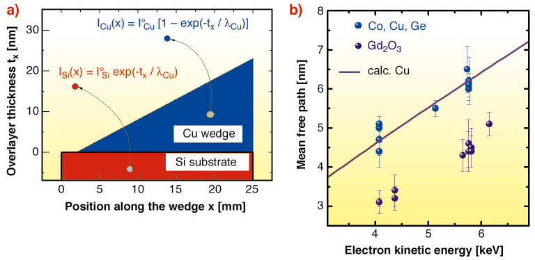
We have also determined ![]() over the 4-6 keV range of electron kinetic energy Ek, using the so-called overlayer method (see Figure 13a), i.e., measuring the intensity of substrate and overlayer core level peaks vs. the overlayer thickness [3]. Experimental values of
over the 4-6 keV range of electron kinetic energy Ek, using the so-called overlayer method (see Figure 13a), i.e., measuring the intensity of substrate and overlayer core level peaks vs. the overlayer thickness [3]. Experimental values of ![]() for Co, Cu, Ge and Gd2O3 are shown in Figure 13b. In the case of Cu, for instance, we find
for Co, Cu, Ge and Gd2O3 are shown in Figure 13b. In the case of Cu, for instance, we find ![]() = 62 Å at Ek = 6 keV, to be compared with
= 62 Å at Ek = 6 keV, to be compared with ![]() = 8 Å at 600 eV. These values lead to some important remarks:
= 8 Å at 600 eV. These values lead to some important remarks:
a) the information depth (defined as the thickness producing 95% of the total signal) is ~ 200 Å at 6 keV, against ~ 24 Å at 600 eV;
b) the contribution to the total intensity coming from the first atomic layer (![]() 2 Å) is 3% at 6 keV and 25% at 600 eV;
2 Å) is 3% at 6 keV and 25% at 600 eV;
c) photoemission from a 10 Å thick layer buried under 100 Å of Cu will still be measurable at 6 keV (~3 x 10⁻² reduction), but not at 600 eV (~3 x 10⁻⁶ reduction).
 |
|
Fig. 13: Experimental determination of the mean free path |
To conclude, our HAXPES measurements on ID16 set realistic conditions for photoemission in terms of both energy resolution and bulk sensitivity. The large probing depth achieved will have an immediate bearing on the measure of electronic properties in strongly correlated systems.
References
[1] I. Lindau, P. Pianetta, S. Doniach and F. Spicer, Nature 250, 214 (1974).
[2] K. Kobayashi et al. Appl. Phys. Lett. 83, 1005 (2003); M. Taguchi et al. Phys. Rev. Lett. 95, 177002 (2005) and refs therein.
[3] M. Sacchi et al., Phys. Rev. B 71, 155117 (2005).
Principal Publication and Authors
P. Torelli (a), M. Sacchi (a), G. Cautero (b), M. Cautero (b), B. Krastanov (b) P. Lacovig (b), P.Pittana (b), R. Sergo (b), R. Tommasini (b), A. Fondacaro (c), F. Offi (c), G. Paolicelli (c), G. Stefani (c), M. Grioni (d), R. Verbeni (e), G. Monaco (e) and G. Panaccione (f), Rev. Sci. Instr.76, 023909 (2005).
(a) Lab.LURE, Centre Univ. Paris Sud, Orsay (France)
(b) Sincrotrone Trieste S.C.p.A. (Italy)
(c) Dip. di Fisica Univ. Roma III (Italy)
(d) EPFL, Lausanne (Switzerland)
(e) ESRF
(f) TASC Laboratory, INFM – CNR, Trieste (Italy)


