- Home
- Users & Science
- Scientific Documentation
- ESRF Highlights
- ESRF Highlights 2016
- X-ray nanoprobe
- An individual strained germanium nanowire probed using a nanofocused X-ray beam
An individual strained germanium nanowire probed using a nanofocused X-ray beam
Low dimensional systems such as nanowires attract significant attention for the development of brighter and more efficient light sources in the infra-red wavelength regime. Researchers are investigating their new opto-electronic properties and trying to control them with miniaturised functional devices.
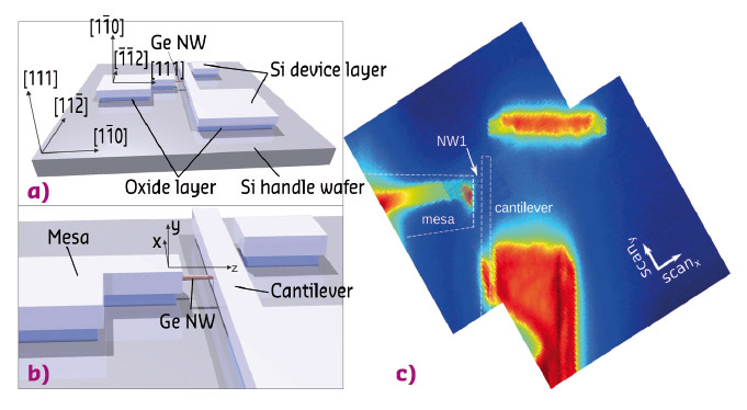
In this work, the lattice plane spacings of individual nanometre sized objects were measured with outstanding precision using synchrotron based X-ray diffraction. Scanning X-ray diffraction (SXRD) microscopy can provide local resolution along the length of these objects, allowing minute changes in strain to be tracked within single nanowires. The wires were grown into a supporting structure between a rigid mesa and a flexible cantilever, as depicted in Figure 38a,b. An oxidation step during sample fabrication allowed the wire to be strained uniaxially by applying a bending force on the cantilever during wire growth, in combination with controlled relaxation afterwards [1,2]. While strain-induced changes of the lattice vibrations were probed using µ-Raman analysis, the underlying strain state was investigated using high-resolution XRD at beamline ID01.
To illuminate only a certain part of a single wire, a beam focused down to 250 nm was used. Due to the sample geometry, XRD data around the (2 0)Bragg spot yields the strain values directly in the direction perpendicular to the wire growth axis (see Figure 38). Finite element method (FEM) calculations were used to estimate the strain in the axial direction. From the diffraction data, the diameter of the crystalline wire core was determined, while scanning electron microscopy data gave the total diameter including a partially-oxidised amorphous Ge shell. Both geometric parameters were used in the FEM model.
 |
|
Fig. 38: Sample sketch overview (a) and close-up (b). c) Resulting real-space map of SXRD microscopy at the Si and Ge (2 |
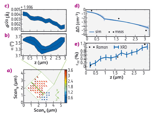
Due to the tapering of the nanowires, i.e., a smaller diameter at the top compared to the bottom, the strain concentrates in the wire tip, as shown in Figure 39a-c. For the axial strain component, very significant values up to εzz = 1.13% have been detected, and a strain gradient was found. Laterally, the wires exhibit a small bend due to shear strains induced by the device geometry (slight twisting of the cantilever due to inhomogeneous oxidation and non-symmetrical growth of the nanowire in the gap). The amorphous shell gives rise to additional stiffening, so that overall a rather complex strain state within a single nanowire is reached.
 |
|
Fig. 39: a) Tilt and bending map of a nanowire, calculated from all Bragg peak positions with respect to the crystallite's Bragg peak (blue dots with 0°), at different real-space positions. The arrows indicate the direction, while the bending values are colour coded. For illustration, the green dashed line indicates the position of the nanowire. Line plots of the measured bending distribution α and the lattice plane spacing d(2 |
From the strain tensor obtained by the XRD/FEM analysis, the expected Raman peak shifts are calculated as a function of position along the nanowire, as shown in Figure 39d,e. They reproduce the experimentally obtained Raman shifts very well. Assuming a uniaxial strain state in the wire (which is not perfectly true but a very good approximation, considering principal and shear strain components from the XRD/FEM results), a linear strain shift coefficient of k = 434 cm between Raman response and the axial strain component, ∆Ω ≡ kεzz, is found, in good agreement with bulk literature values [3], indicating that the elastic response of the Ge nanowires is very much bulk-like even at such considerable levels of strain.
In summary, XRD/FEM results are corroborated by a µ-Raman analysis using a linear relationship between uniaxial strain and line shift of single Ge nanowires. Moreover, they allow additional insight to be obtained into the full strain state of the nanowires thanks to a nanofocused X-ray beam.
Principal publication and authors
Strain distribution in single, suspended germanium nanowires studied using nanofocused X-rays, M. Keplinger (a), R. Grifone (a,b,c), J. Greil (d,e), D. Kriegner (a,f), J. Persson (g,h), A. Lugstein (d), T. Schülli (b) and J. Stangl (a), Nanotechnology 27, 055705 (2016); doi: 10.1088/0957-4484/27/5/055705.
(a) Institut für Halbleiter- und Festkörperphysik, Johannes Kepler Universität Linz (Austria)
(b) ESRF
(c) DESY-Photon Science, Deutsches Electronen-Synchrotron, Hamburg (Germany)
(d) Institute of Solid State Electronics, Vienna University of Technology (Austria)
(e) Department of Applied Physics, Eindhoven University of Technology (Netherlands)
(f) Faculty of Mathematics and Physics, Charles University, Prague (Czech Republic)
(g) Center for Electron Nanoscopy, Technical University of Denmark, Lyngby (Denmark)
(h) Gemeinschaftslabor für Elektronenmikroskopie, RWTH Aachen (Germany)
References
[1] A. Lugstein et al., Nano Letters 10, 3204–3208 (2010).
[2] J. Greil et al., Nano Letters 12, 6230–6234 (2012).
[3] F. Cerdeira et al., Phys. Rev. B 5, 580–593 (1972).
 0) Bragg reflections. The cantilever and parts of the mesa (white dashed lines) are not visible, i.e. not in Bragg condition due to their torsion and bending.


