- Home
- News
- Spotlight on Science
- Revealing the local...
Revealing the local structure of a fully operable infrared sensor under cryogenic conditions
06-10-2021
In-situ dark-field X-ray microscopy (DFXM) has been used to investigate the structural modifications in an HgCdTe-based infrared sensor. While the temperature-induced strain remained elastic, the indium bumps were considered as stress concentration zones due to their anisotropic thermal expansion behaviour.
HgCdTe, or mercury cadmium telluride (MCT), is today’s material of choice for developing high-performance infrared (IR) detectors covering a broad range of applications from astronomy to gas monitoring. Despite the improvements in performance of these sensors in the last decades, device failure due to the lattice and thermal expansion mismatches between MCT and the silicon readout circuit still affects the overall performance.
Today, the physical origin of defective photodiodes is a field of intense research. The investigation of epitaxial mismatch strain between the MCT layer and the CdZnTe (CZT) substrate is of particular interest [1,2], as is the impact of the different processing steps during device fabrication, such as etching, ion implantation, surface passivation, metallisation and annealing.
Moreover, the thermal mismatch between MCT and the Si readout circuit in 2D Focal Plane Arrays (FPAs) is another source of defective photodiodes, since these sensors typically operate at 80 K. While material issues at the wafer scale can be addressed through conventional techniques, technological processes resulting in pixel failures require more localised probes. Recently, Laue micro-diffraction was employed to determine localised strain fields in MCT during the fabrication of individual diodes [3], yet with a rather narrow field of view (one or two pixels at most) and with limited spatial resolution.
To overcome these drawbacks, dark-field X-ray microscopy (DFXM) was used at beamline ID01 to reveal the structural distortions in a fully operably MCT sensor at operating temperatures. DFXM is a non-destructive, diffraction-based imaging technique that allows mapping of strain and orientation in embedded crystals with high spatial and angular resolution reaching up to 50 nm and 0.001°, respectively [4,5].
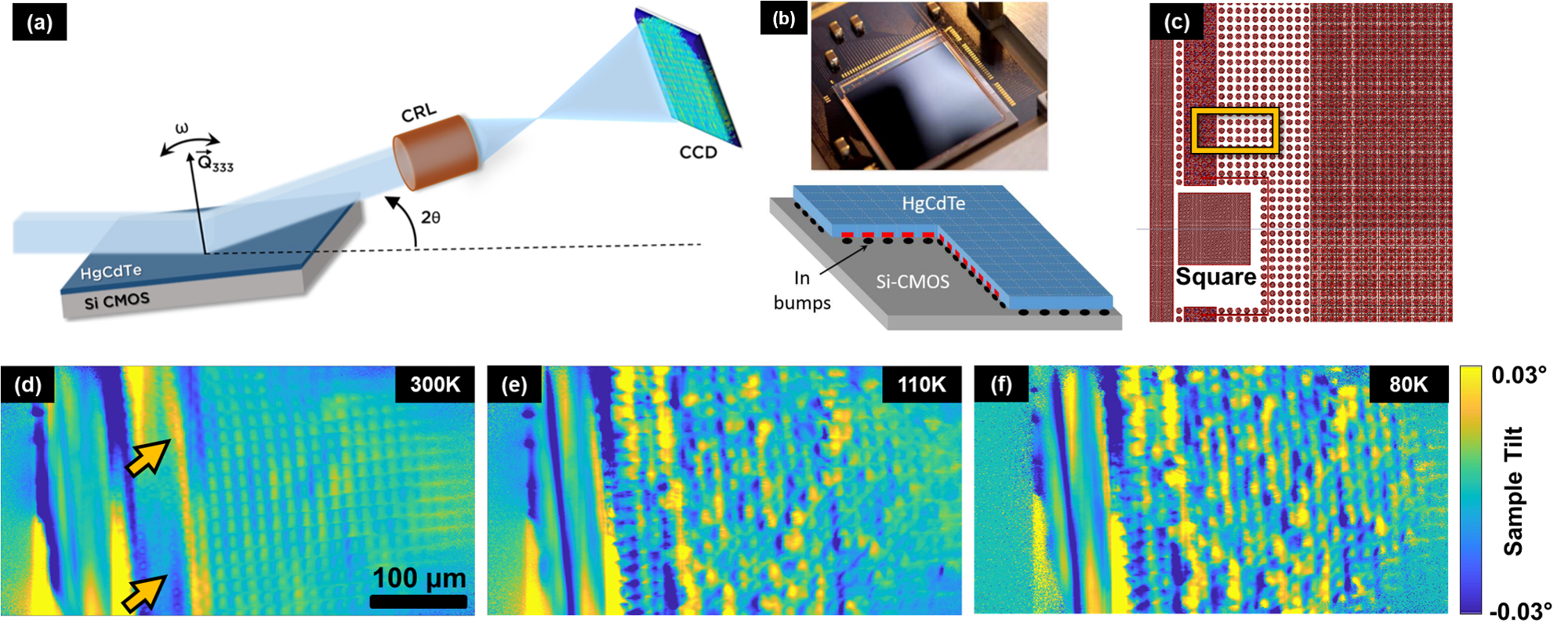
Fig. 1: a) DFXM experimental setup. The X-ray objective compound refractive lens (CRL) is placed along the diffracted beam to magnify the projection of the diffracting MCT crystal. b) Photo and the schematics of the device showing the different layers of the overall design. c) The architecture of the same area in terms of implantation and contact structure. The yellow rectangle shows the regions studied with DFXM. Reconstructed peak position maps of the sample orientation at (d) 300 K, (e) 110 K and (f) 80 K. The yellow arrows in (d) show the round-shaped mechanical contacts, which are found at the left side of the yellow square in (c).
This work investigated the nanoscale structural evolution over a large population of photodiodes down to operating temperature (80 K). The strain and orientation states of MCT pixels were studied comprehensively at various length scales (Figure 1). The results show an increase in the axial strain of the MCT pixels upon cooling. The measured stress is reported to be below 30 MPa, thus in the elastic regime, and completely reversible through a full temperature cycle (Figure 2). This experiment shows, for the first time, the strain evolution of individual pixels with quantitative statistical information over a 5 mm distance within an operable IR sensor.
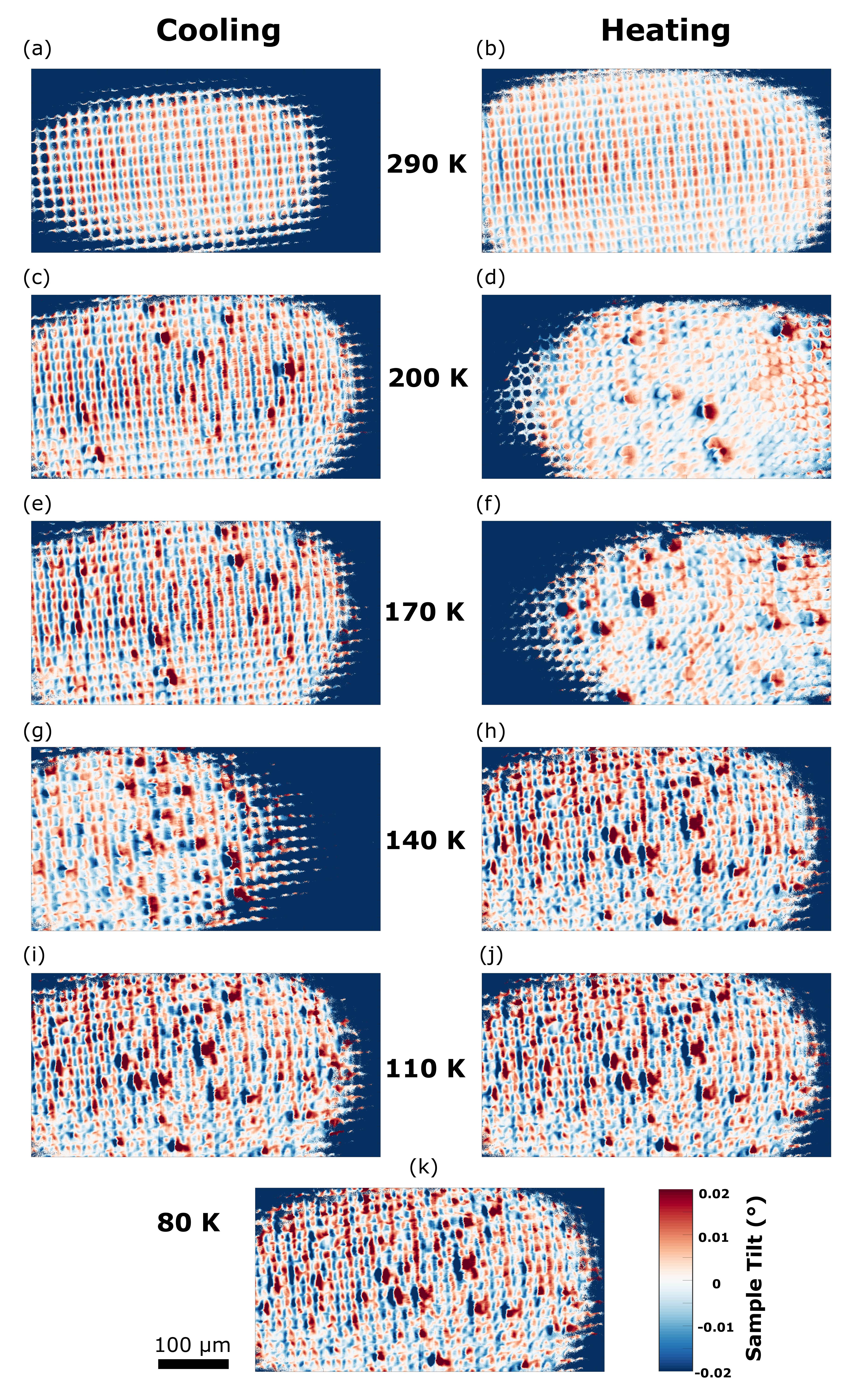
Fig. 2: Orientation maps during the temperature cycle, cooling down to 80 K and heating back up to room temperature.
Moreover, this work presents the first successful proof-of-concept study for DFXM investigations under cryogenic conditions. The post-DFXM electrical characterisation showed that the IR sensor was still operable after the X-ray beam exposure. The DFXM studies were complemented with Finite Element Modelling (FEM) analyses to assess the nature of the tension-compression doublets appearing below 200 K. The anisotropic coefficient of thermal expansion of In bumps that link the MCT pixels and the Si readout circuit results in the formation of doublets (regions of ~30-40 µm coupled with compression and tension contributions) due to random crystallographic orientations of the In bumps beneath the MCT layer.
These results illustrate the capabilities of DFXM in IR detector studies and open up new avenues for further studies in which several thermal cycles can be applied in operando conditions, along with an electrical field. The outcome of this work should help to improve IR sensor quality and functionality at real operating conditions, which will allow for new insights into the strain state of the HgCdTe layer of IR sensors and validation of structural models.
Principal publication and authors
In-situ mapping of local orientation and strain in a fully operable infrared sensor, C. Yildirim (a,b) D. Brellier (a), R. Pesci (c), F. Boulard (a), N. Baier (a), T. Zhou (b), T. Nguyen-Thanh (a), P. Gergaud (a), T. Schulli (b), P. Ballet (a), Acta Mater. 220, 117292 (2021); https://doi.org/10.1016/j.actamat.2021.117290
(a) Université Grenoble Alpes CEA, Leti, Grenoble (France)
(b) ESRF
(c) ENSAM-Arts et Métiers Sciences and Technologies, Metz (France)
References
[1] C. Yildirim et al., J. Synchrotron Radiat. 28, 1 (2021).
[2] P. Ballet et al., J. Cryst. Growth 371, 130 (2013).
[3] A. Tuaz et al., J. Electron. Mater. 46, 5442 (2017).
[4] H. Simons et al., Nat. Commun. 6, 6098 (2015).
[5] S. Leake et al., J. Synchrotron Radiat. 26, 2 (2019).
partners


European Synchrotron Radiation Facility - 71, avenue des Martyrs, CS 40220, 38043 Grenoble Cedex 9, France.