- Home
- News
- Spotlight on Science
- X-ray imaging analysis...
X-ray imaging analysis of structural defects in silicon contaminated with carbon
01-06-2023
Carbon impurities can affect the electrical performance of silicon, which is widely used in the production of photovoltaic solar cells. The impact of the presence of carbon on the generation of distortions and defects in crystalline silicon was studied in situ, during solidification and ex situ using X-ray imaging at beamlines ID19 and BM05.
Grain boundaries, dislocations and impurity contamination control during solidification constitute major challenges in silicon photovoltaic cell manufacturing processes. Carbon is one of the most frequent impurities in directional solidification processes. It can be introduced due to the industrial furnace environment, crucible and starting feedstock, in particular in the case of recycled materials. Carbon can be at the origin of shunts, several-scale defects and distortions in the crystal that can all contribute to a degradation of the final performance of the solar cells.
In this work, the dynamics of the growth mechanisms involved in the formation of the grain structure and of defects related to the presence of carbon in silicon was studied using a combination of in-situ X-ray radiography and X-ray white beam Bragg diffraction imaging (topography) at beamline ID19 [1]. The results showed that the grain structure originating from solidification constitutes of a higher proportion of high-order twin (δ in Figure 1) and of random angle grain boundaries for carbon-contaminated samples, compared with pure samples. This is due to the higher probability, in the presence of carbon and related precipitates, of grain nucleation not all related to the energetically Σ3 twin most favourable nucleation in pure samples. Such twin boundaries are at the origin of grain-scale (mm to cm) distortions in the crystal that persist and are accentuated after cooling down. They may also be at the origin of dislocation emission and act as preferential sites for the segregation of impurities in general.
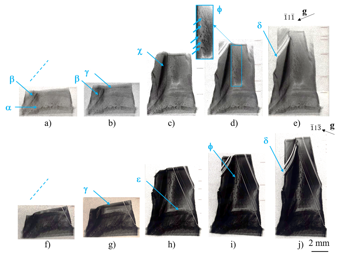
Fig. 1: Sequence of topographs during solidification of a silicon reference sample contaminated with carbon (1.5 x 10¹⁷ at/cm3) for the 1 ̅11 ̅ (top) and 1 ̅13 ̅ (bottom) diffraction spots. a) and (f) t0: start of cooling-down at -1 K/min; (b) and (g) t0 + 6 min; (c) and (h) t0 + 9 min; (d) and (i) t0 + 11 min; (e) and (j) t0 + 14 min.
In order to obtain a more precise analysis of defects, including sub-grains, and to quantify their distortion fields and misorientations, ex-situ Rocking Curve Imaging (RCI) experiments were conducted at beamline BM05 after solidification of the samples. Both in-situ (Φ in Figure 1) topography experiments and ex-situ RCI experiments (Figure 2) showed that local distortion regions of the crystalline structure associated to sub-grains were present, not only on the surface of the samples and ingots, but also within the bulk of the samples. The defects were observed during solidification of different types of samples containing carbon (mono-crystal, industrial ribbons and multi-crystalline sample) and were retrieved after solidification.
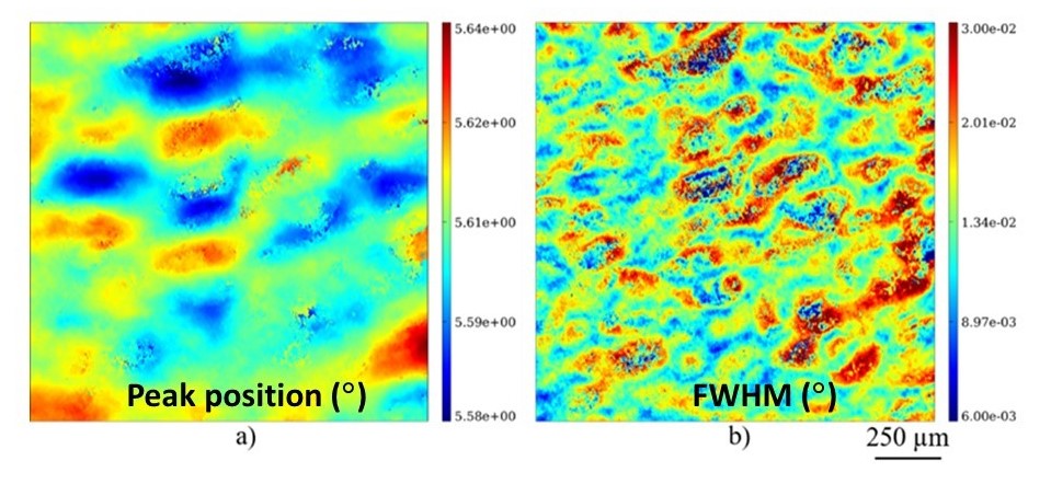
Fig. 2: Same sample as in Figure 1 after solidification: projection RCI ({111} diffraction spot) results with a pixel size of 0.75 µm, a field of view of 1.5 x 1.5 mm2 and a Bragg angle: θB= 5.6°. a) Peak-Position (PP) map. The scale gives the position of the peak in degree. b) Full Width Half Maximum (FWHM) map. The scale gives the misorientation value in degree.
The results suggested a mechanism on how these features are formed during solidification in the presence of SiC precipitates at the level of the solid-liquid interface. The growing silicon just above the precipitates is misoriented compared to the solid-liquid interface of silicon growing from the seed. When both regions meet, sub-grains result and compete with each other due to the presence of precipitates all over the sample volume. Bunches of dislocations can also be directly related to the presence of carbon precipitates thanks to the in-situ topography imaging.
The study demonstrates the major influence of carbon on the formation of the grain structure and crystalline defects at different scales while growing silicon. These growth features, which remain after solidification, have a severe impact on the electrical properties of silicon, and thus on the performance of photovoltaic solar cells. The correlation of both in-situ and ex-situ diffraction imaging techniques implemented at the ESRF was fundamental for the success of this study.
Principal publication and authors
Crystal distortions and structural defects at several scales generated during the growth of silicon contaminated with carbon, H. Ouaddah (a), G. Regula (a), G. Reinhart (a), I. Périchaud (a), F. Guittonneau (b), L. Barrallier (b), J. Baruchel (c), T.N. Tran Caliste (c), N. Mangelinck-Noël (a), Acta Mater. 252, 118904 (2023); https://doi.org/10.1016/j.actamat.2023.118904
(a) Aix Marseille Université, Université de Toulon, CNRS, IM2NP, Marseille (France)
(b) Arts et Métiers Institut de Technologie, HESAM 2, Cours des Arts et Métiers, Aix-en-Provence (France)
(c) ESRF
Reference
[1] M. Becker et al., J. Appl. Cryst. 52(6), 1312-1320 (2019).
| About the beamlines: ID19 and BM05 |
|
Beamline ID19 of the ESRF operates experimental facilities located 150 m downstream of the source: the long distance suppresses the influence of the finite sources size on the image formation and hence, allows one to exploit propagation-based phase contrast. Frequently, polychromatic configurations are applied as the increased bandwidth leads to drastically reduced exposure times, down to the nanosecond regime for selected applications. Fast tomography and ultra-high-speed radiography are frequently coupled with sample environments at beamline ID19. Besides classical tomography furnaces and a cold cell, recent installations include different kinds of presses for uni-axial and tri-axial load, dynamic compression installations such as a mesoscale gas launcher, a Split-Hopkinson pressure bar and pulsed laser as well as dedicated rigs for battery abuse testing and additive manufacturing in situ.
|
partners


European Synchrotron Radiation Facility - 71, avenue des Martyrs, CS 40220, 38043 Grenoble Cedex 9, France.