- Home
- News
- Spotlight on Science
- Dark-field X-ray...
Dark-field X-ray microscopy for microelectronics: revealing fatigue mechanisms in copper layers
26-06-2023
Dark-field X-ray microscopy has been used at beamline ID06-HXM to analyse copper metallisation layers used in the circuits of microelectronic devices, revealing microscale damage mechanisms caused by heating during use. The insights revealed could aid the design of more efficient, longer-lasting devices.
With increasing demands in efficiency and power density, ensuring the lifetime of integrated circuits for microelectronic devices is becoming ever more challenging. In such devices, metallisation layers are implemented as current and heat conduction pathways and are often manufactured from materials such as copper (Cu), which suffers from a low thermal microstructural stability. Particularly in high-power applications, devices heat up and cool down repeatedly, inducing a cyclical mechanical load that may result in material fatigue and eventually device failure, thereby effectively limiting the device lifetime.
In this context, the microstructure of specially designed Cu metallisation test chips that can be thermo-mechanically cycled in a short span of time was analysed using a combination of advanced complementary techniques. Dark-field X-ray microscopy (DFXM) was used at beamline ID06-HXM to provide insights at the grain level, while scanning electron microscopy (SEM) was used to track the overall evolution of the granular film microstructure and X-ray nanotomography (at DESY) revealed volumetric data on the percolation of voids at various stages.
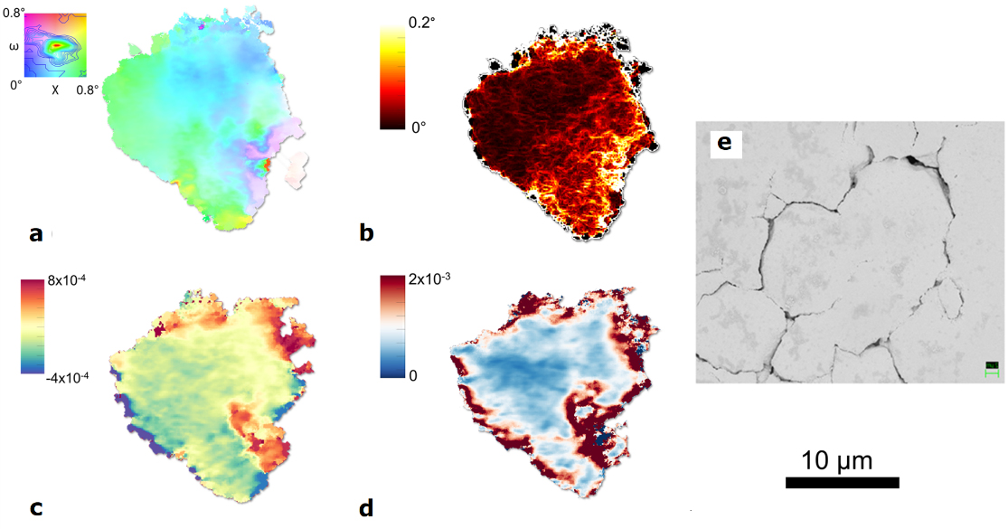
DFXM is a comparatively new technique at ID06-HXM [1], where a coherent monochromatic X-ray beam is focused on a sample, and an objective compound refractive lens is then placed in an appropriate position to magnify a diffracting feature such as a single grain onto a position-sensitive detector. By tilting the sample very precisely through various angles while recording the detector images, quantities such as crystal mosaicity, misorientation, strain and defect concentrations (Figure 1) can be mapped within the individual grain.
Click image to enlarge
Fig. 1: Maps reconstructed from DFXM data showing a Cu grain cycled 50k times: (a) depicts the mosaicity of the crystal lattice; in (b) the kernel-average misorientation indicates the diffuse variation of the diffraction vector; (c) shows the relative axial strain, corresponding to the distribution of 2nd order X-ray elastic strain, and (d) presents the breadth of the diffraction peak, i.e., the concentration of lattice defects. A SEM micrograph of the same grain is shown in (e); the different grain shapes are due to the fact that in DFXM the entire volume of the grain is analysed, while SEM is surface-sensitive.
The experiment employed a thermo-mechanical cycling procedure of heating up to 400°C from a baseline temperature of 100°C, with pulses of 200 µs in length and a heating rate of 106 K/s, at a repetition rate of 1 Hz and up to 50 000 times. This resulted in significant microstructural changes in the samples, which consisted of 20 µm-thick Cu films electro-deposited onto the polysilicon heating structure of the test chips.
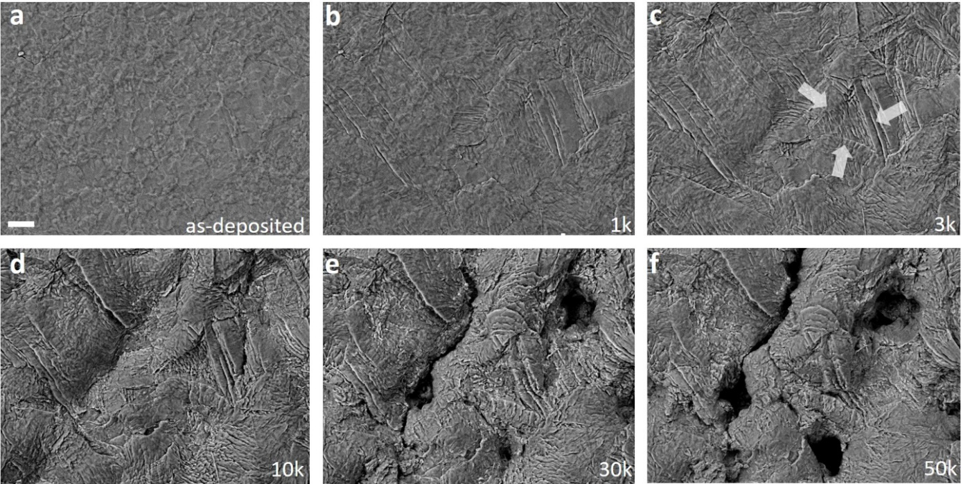
As illustrated by SEM images in Figure 2, the Cu film surface is significantly roughened as cycling progresses. From the earlier stages of cycling, it is evident that the roughening is due to accumulated small-amplitude plastic deformation, which initially takes the form of slip marks at the film surface, later compounding into protrusions and intrusions over time. At very high cycle numbers, elongated valleys and round-shaped voids become visible. These severe microstructural changes are well-known to be accompanied by a degradation in the functional properties of the Cu film [2], such as electrical resistance.
Click image to enlarge
Fig. 2: SEM images of the surface of the tested Cu film after various numbers of thermal cycles. The scale bar in (a) is 10 µm long. Along with an increase in roughness starting at low cycles, voids also eventually form, percolating through the entire thickness of the film and thereby increasing electrical sheet resistance. Arrows in (c) indicate a Cu grain, where further deformation in the grain interior is comparatively hindered, while the surrounding regions continue to deform.
Interestingly, on certain parts of the surface, comparatively stable structures remain visible throughout many cycles, as marked by arrows in Figure 2c. Correlation with DFXM results revealed the large differences in deformation behaviour between the Cu grain interior and the grain boundaries. It was shown that the residual strain and orientation gradients initially present inside Cu grains are homogenised by thermo-mechanical cycling, while at the grain boundaries they pile up along with newly introduced lattice defects (Figure 1a-d).
In terms of materials science, this is interpreted as deformation-induced recovery in the Cu grain interior, accompanied by hardening and embrittlement at Cu grain boundaries. Future recipes for Cu metallisation synthesis will be able to take these new insights into account, diminishing their impact on functional performance and boosting the lifetime of microelectronic devices. Furthermore, with the advantages offered by the ESRF-EBS upgrade, operando experiments providing even greater detail are now possible for the investigation of the intra-granular dynamics of microelectronic metallisation layers.
Principal publication and authors
Intragranular Thermal Fatigue of Cu Thin Films: Grain Boundary Hardening, Strain Localization and Voiding, K. Hlushko (a,b), T. Ziegelwanger (a), M. Reisinger (c), J. Todt (a), M. Meindlhumer (a), S. Beuer (d), M. Rommel (d), I. Greving (e), S. Flenner (e), J. Kopeček (f), J. Keckes (a) C. Detlefs (g), C. Yildirim (g), Acta Mater. 253, 118961 (2023); https://doi.org/10.1016/j.actamat.2023.118961
(a) Department of Materials Science, Montanuniversität Leoben, Leoben (Austria)
(b) Materials Center Leoben Forschung GmbH, Leoben (Austria)
(c) KAI – Kompetenzzentrum Automobil- und Industrieelektronik GmbH, Villach (Austria)
(d) Fraunhofer Institute for Integrated Systems and Device Technology IISB, Erlanger (Germany)
(e) Institute of Materials Physics, Helmholtz Zentrum Hereon, Geesthacht (Germany)
(f) FZU – Institute of Physics, Czech Academy of Sciences, Praha (Czech Republic)
(g) ESRF (France)
References
[1] M. Kutsal et al., IOP Conf. Ser. Mater. Sci. Eng. 580, 012007 (2019).
[2] S. Moser et al., Microelectron. Reliab. 137, 114782 (2022).
| About the beamline: ID06-HXM |
|
ID06-HXM is a hard X-ray microscopy beamline for the study of a wide range of materials, ranging from structural materials such as metals and alloys to functional materials such as ferroelectrics to biominerals. The main technique offered is dark-field X-ray microscopy (DFXM). DFXM is a full-field imaging technique for non-destructive mapping of the structure, orientation and strain of deeply embedded crystalline elements in 3D. The instrument at ID06-HXRM is designed to combine DFXM with coarse-scale 3D grain-mapping techniques such as 3D X-ray diffraction (3DXRD) and diffraction contrast tomography (DCT), as well as classical tomography and diffraction topography. This combination enables the user to rapidly progress from fast overviews of the entire specimen to detailed studies of local phenomena in a single experimental setting, without the need to dismount the sample. |
partners


European Synchrotron Radiation Facility - 71, avenue des Martyrs, CS 40220, 38043 Grenoble Cedex 9, France.