- Home
- News
- Spotlight on Science
- Decoding the origin...
Decoding the origin of UV emission in Zn2GeO4/SnO2 nanowire heterostructures
23-08-2023
Spatially resolved X-ray nano-analysis performed at beamline ID16B revealed the connection between impurities, secondary phase formation and asymmetrically distributed UV emission in a Zn2GeO4/SnO2 nanowire heterostructure. These findings lay the foundation for the development of nano-heterostructures with tailored spectroscopic properties, which could be highly beneficial for optoelectronic applications.
Hybrid semiconductor nanowire heterostructures are an ideal playground for cutting-edge optoelectronic nanodevices. Among the several synthesis methods, Plateau-Rayleigh crystal growth is an effective route for producing decorated nanowires with unprecedent properties [1]. Unconventional morphological characteristics with modulations in periodicity, size and cross-sectional anisotropy are produced by controlling the deposition conditions. Although lateral variations in composition and/or crystal structure are thought to play a key role in their optical response, it has been challenging to simultaneously investigate the elemental ordering, atomic arrangement and light emission at length scales of tens to hundreds of nanometers.
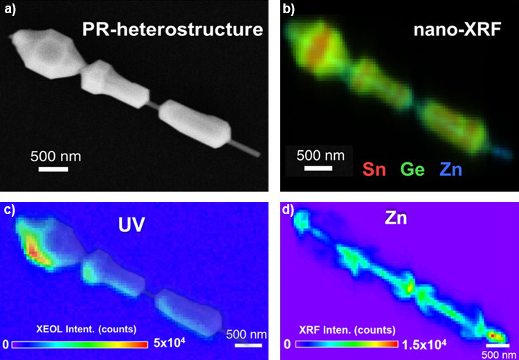
Traditionally, electron microscopy is used to study the formation of clusters and imperfections in representative cross-sections of samples. However, in this work, a complete spatially resolved X-ray nano-analysis was performed at beamline ID16B to correlate the crystal symmetry, chemical composition and optical properties of an entire Zn2GeO4/SnO2 nanowire heterostructure produced by Plateau-Rayleigh instability (Figure 1a). X-ray fluorescence (XRF), X-ray excited optical luminescence (XEOL), X-ray diffraction (XRD) and X-ray absorption (XAS) were simultaneously utilised to investigate the heterostructure at the nanoscale. This ‘all-in-one’ strategy, which makes use of a hard X-ray nanobeam, provides a complete correlative image of a single decorated nanowire.
Click image to enlarge
Fig. 1: a) Scanning electron microscopy (SEM) image of Plateau-Rayleigh heterostructure. b) XRF map in RGB visualisation that depicts the XRF intensities of Sn (red), Ge (green), and Zn (blue). c) XEOL integrated intensity map over the UV range. d) XRF map depicting the XRF intensity of Zn in the P-R heterostructure.
By using a combination of synchrotron nano-analysis techniques, it was possible to identify the origin of the asymmetric UV emission in the heterostructure. First, nano-XRF measurements revealed that the crystallites decorating the nanowire are composed of Zn-doped Sn1-xGexO2. The significant inclusion of Ge in the SnO2 crystallites suggests that an alloy has been formed, which could significantly alter the structural order. However, no evidence of a one-to-one connection between the Ge and Sn distributions was found. The Ge atoms are preferentially located within the conical faceted sides of the crystallites (sandwich-like structure compared to Sn, as illustrated in Figure 1b), which may result in the creation of secondary phases or defects, and consequently impact the spatial distribution of the carrier recombination processes. These Zn-doped Sn1-xGexO2 crystallites exhibited an asymmetrically distributed XEOL UV emission (Figure 1c), which was collected only in the areas with the highest Zn impurity content (Figure 1d), suggesting the existence of new electronic states assisted by Zn complexes.
Click image to enlarge
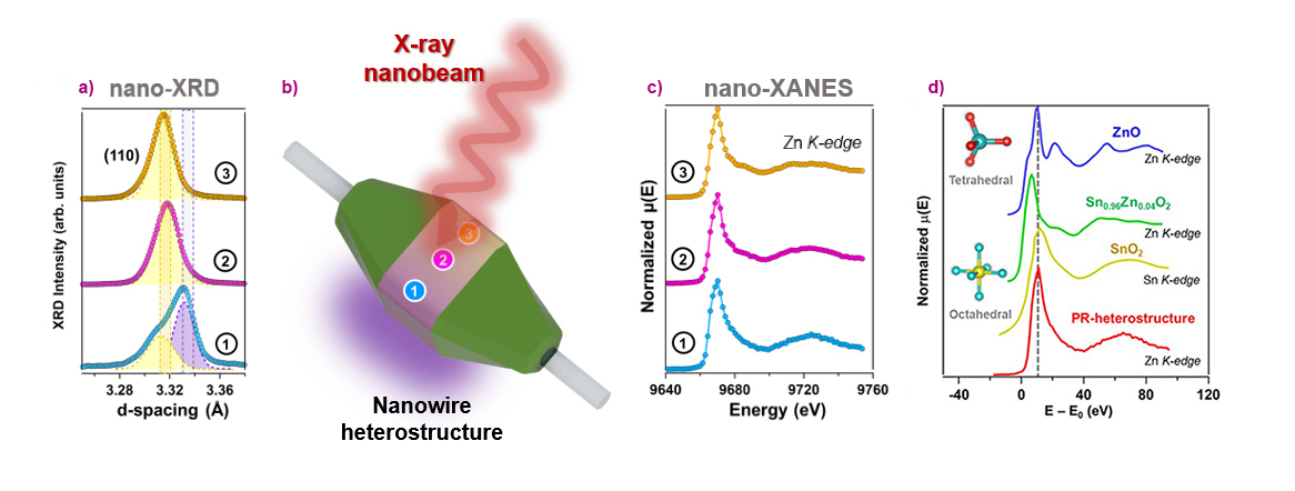
Fig. 2: a) XRD pattern of the (110) reflection acquired at three different areas of the sample, indicated by numbers in the sketch shown in (b). c) XANES data around the Zn K-edge taken in the same three sample areas where XRD measurements were acquired. d) XANES data recorded around the Zn or Sn K-edges of reference materials with tetrahedral (ZnO), distorted octahedral (Sn0.96Zn0.04O2) and octahedral (SnO2) coordination, in addition to the one acquired in the PR heterostructure (at the bottom of the graph).
In addition to chemical composition, secondary phases that form due to changes in crystal structure can have a significant impact on the optical properties and optoelectronic performance of materials. The XRD results (Figures 2a-b) suggest that a secondary crystalline phase exists in the regions with the highest Zn concentrations. Zn atoms replace Sn atoms in the rutile crystal lattice, as shown by the X-ray absorption near-edge structure (XANES) findings (Figures 2c-d). Therefore, the results suggest that a Zn impurity-assisted process may be responsible for the UV optical emission, which involves the formation of a secondary phase within the Sn1-xGexO2 crystallites.
This work demonstrated that a multimodal synchrotron nanoprobe is a comprehensive and effective approach for gaining a thorough understanding of complex nanoscale hybrid systems at the atomic and electronic levels. The findings shed light on unknown underlying mechanisms that are essential for tailoring emergent properties for the rational design of new complex nanodevices based on one-dimensional materials.
Principal publication and authors
Interplay between Crystal Structure and Optical Response in Plateau–Rayleigh Zn2GeO4/SnO2 Heterostructures, J. Dolado (a), F. Malato (b), J. Segura-Ruiz (a), R. Martínez-Casado (c), M. Taeño (c), I. Snigireva (a), P. Hidalgo (c), B. Méndez (c) and G. Martínez-Criado (a,b), Adv. Photon. Res. 2300063 (2023); https://doi.org/10.1002/adpr.202300063
(a) ESRF
(b) ICMM, CSIC, Madrid (Spain)
(c) Materials Physics Department, Universidad Complutense de Madrid, Madrid (Spain)
References
[1] R.W. Day et al., Nat. Nanotechnol. 10(4), 345-352 (2015).
[2] J. Dolado et al., Cryst. Growth Des. 20(1), 506-513 (2019).
| About the beamline: ID16B |
|
ID16B is a hard X-ray nanoprobe dedicated to 2D or 3D analysis of nano-scaled materials combining X-ray fluorescence (XRF), diffraction (XRD), absorption spectroscopy (XAS), excited optical luminescence (XEOL), X-ray beam induced current (XBIC) and phase-contrast imaging. Low temperature, in-situ or operando sample environments can be accommodated. ID16B is dedicated to research areas with high scientific and societal impacts such as nanotechnology, earth and environmental sciences, and bio-medical research. |


