- Home
- Users & Science
- Scientific Documentation
- ESRF Highlights
- ESRF Highlights 2001
- Collective Atom Dynamics
- Evidence of Friedel Oscillations in Quasi-one-dimensional Conductors
Evidence of Friedel Oscillations in Quasi-one-dimensional Conductors
Low dimensional, and in particular quasi-one-dimensional (1D) conductors, have been the object of extensive studies in the past. Their peculiar properties are intimately related to the instability of the 1D electron gas, which leads, through electron-phonon coupling, to the stabilisation of a periodic lattice distortion at the Peierls transition. The period of the corresponding modulation of the electronic density, the so-called charge-density wave (CDW), is the inverse of twice the Fermi wave vector kF, which is in general not an integer multiple of the underlying crystal lattice. In real crystals, this incommensurate CDW is pinned by crystal defects, such as impurity atoms, giving rise to local modifications of the electron density, the Friedel oscillations (FO). These can be seen as a result of the screening of the impurity charge by the conducting electrons. Detailed information on the FO's and the pinning can be obtained by an intensity and profile asymmetry analysis of the X-ray diffraction CDW satellite reflections.
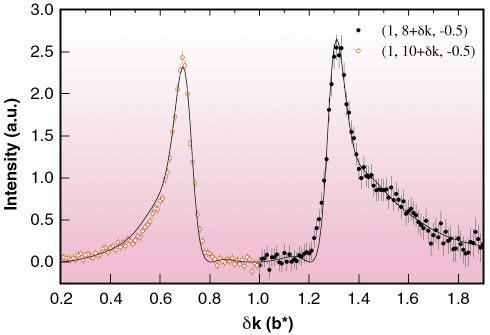
We have performed experiments on BM2, the French CRG D2AM beamline, on heavily vanadium-doped (2.8 at % V) blue bronzes (K0.3MoO3). These quasi-one-dimensional materials consist of clusters of ten octahedra MoO6 stacked along the b direction of the monoclinic lattice. Below its Peierls transition (TP =183 K), satellite reflections appear at a reduced wave vector qc = (1, 0.748, 0.5). We have carefully measured the profile of pairs of ±qc-satellite reflections at low temperature along the chain direction b* (Figure 85). The widths of these reflections are much larger that the experimental resolution (0.008 Å-1 along b*), indicating the loss of the CDW long-range order. From the excess width, the CDW correlation length along the chains was estimated to be lb* = 28.7 Å at 15 K, corresponding roughly to the average distance between impurities. Also, Figure 85 clearly reveals profile asymmetries of the satellite reflections, not observed in pure materials, which we interpret to be due to FO around the V impurities.
 |
Fig. 85: High-resolution profile of the ±qc-satellite reflection at 60 K. The solid line corresponds to the Fourier transform of the FO/CDW distortion shown in Figure 86. |
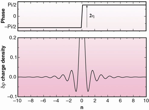
In order to understand the unusual diffraction profiles of Figure 85, we have modeled the distortion around the Vanadium defect by a CDW/FO structure. In 1D, the oscillating part of the electronic density, , around an impurity of charge Z, located at x = 0 (Figure 86a), reads:
(x) = exp(-|x|/
)cos(2kF|x|+
)/|x|,
where is the damping length, and
the phase shift of the electronic wave function at the Fermi level.
is related to Z by the sum rule Z = (2/
)
. Physically, this relation means that the additional charge Z has to be screened by the conduction electrons by bringing a charge of opposite sign into the vicinity of the impurity. In blue bronze, the V5+ atom provides a negative charge (Z = 1) with respect to the molybdenum Mo6+ background, and the induced phase shift amounts to
=
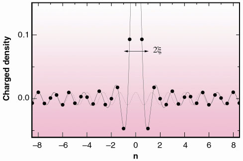
/2. Figure 86b shows a tentative representation of the CDW/FO structure. In a tiny 2
= 16 Å distance around the defect, the FO dominates the charge modulation while at larger distance the CDW is recovered (dotted line). The Fourier transform of this FO/CDW model fits reasonably well with the experimental scattering, especially its asymmetric parts. It is important to point out that the asymmetry effect is due to the phase shift
of the FO, while the regular part of the peak is due to the CDW.
 |
Fig. 86: a) Representation of a pure Friedel oscillation. b) Oscillating part of the hole charge density around an impurity placed at the origin, as a function of the unit cell index n. Circles represent the Mo atoms. |
 |
In summary, our results provide convincing evidence of Friedel oscillations in the vicinity of vanadium impurities in blue bronze. Additional experiments on crystals with different doping levels are planned in order to elucidate more quantitatively the microscopic features of the CDW pinning in low-dimensional materials.
References
[1] For a review, see C. Schlenker, Low-Dimensional Electronic Properties of Molybdenum Bronzes and Oxides, Kluwer Academic, Dordrecht, p. 159 (1989), and J.-P. Pouget, ibid., p. 87.
Principal Publication and Authors
S. Ravy (a), S. Rouzière (a), J.-P. Pouget(a), S. Brazovskii (b) and J.-F. Bérar (c), Phys. Rev. B 62, R16231 (2000).
(a) Laboratoire de Physique des Solides, CNRS UMR8502, Université Paris-Sud, Orsay (France)
(b) Laboratoire de Physique Théorique et Modèles Statistiques, CNRS UMR 8626, Université Paris-sud, Orsay (France)
(c) Laboratoire de Cristallographie CNRS, Grenoble (France)


