- Home
- Users & Science
- Scientific Documentation
- ESRF Highlights
- ESRF Highlights 2002
- X-ray Imaging
- X-ray Standing Wave Microscopy: Chemical Microanalysis with Atomic Resolution
X-ray Standing Wave Microscopy: Chemical Microanalysis with Atomic Resolution
Today's technology and technology-driven research are closely linked to the development of 1-, 2-, and 3-dimensional solid-state structures with length scales ranging from several nanometres for electronic quantum wells to several micrometres for optoelectronic devices, photonic crystals, or micro electro-mechanical systems.
Our development of X-ray Standing Wave (XSW) technique [1] should contribute towards the determination of such structures. XSW is a microscopic technique where we are able to determine the crystalline organisation with subatomic resolution and chemical sensitivity. Moreover, we can exploit its phase sensitivity to characterise materials that exhibit microscopic heterogeneity of their crystallographic polarity.
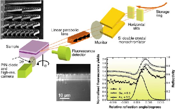
A micro-XSW setup was realised at beamline ID22 (Figure 109). Both, the low angular beam divergence (10 µrad vertically and 20 µrad horizontally) and the small angular source size (2 µrad vertically by 40 µrad horizontally) are necessary conditions to create a monochromatic beam with a low dispersion which can be further focussed by means of a linear refractive lens [2]. With this, an X-ray beam was produced having the dimensions of 1.5 micrometres vertically and 100 micrometres horizontally, with low horizontal divergence.
 |
|
Fig. 109: X-ray standing wave setup for microscopic resolution. The upper left inset shows a set of linear refractive lenses; for this experiment type (c) was used. The high-resolution topogram (lower left inset) reveals the AlGaAs layer, which has a slightly different lattice constant than the GaAs substrate. The micro-XSW measurement on the AlGaAs-layer is shown in the right inset. Reflectivity, fluorescence yields and XSW-fits to the fluorescence yields are displayed as a function of the reflection angle. |
We analysed a GaAs/AlGaAs/GaAs(001) multilayer structure, nowadays important for quantum-well systems with various applications. Via molecular beam epitaxy, a GaAs buffer layer was grown onto the (001) oriented GaAs-wafer surface, followed by a 4 µm layer of AlGaAs (10% Al), and a 4 µm cap layer of GaAs doped with Si. We studied the adjacent layers in cross-section, after cleaving the wafer along the (110) planes (Figure 109). The micro-XSW scans inside the AlGaAs layer and a fit to the measured fluorescence yields (Al K-lines, Ga and As L-lines) reveals the coherent positions P and coherent fractions F of the constituents relative to the AlGaAs (220) planes with FAl = 0.71 ± 0.14, PAl = 0.08 ± 0.04, FAs = 0.62 ± 0.06, PAs = 0.06 ± 0.02, FGa = 0.59 ± 0.04, and PGa = 0.98 ± 0.02. The positions are in agreement with an undistorted lattice of GaAs-type. However, the coherent fractions differ significantly from their ideal value, which would be about 0.94 owing to thermal vibrations indicating some random displacement of the atoms from their ideal lattice positions.
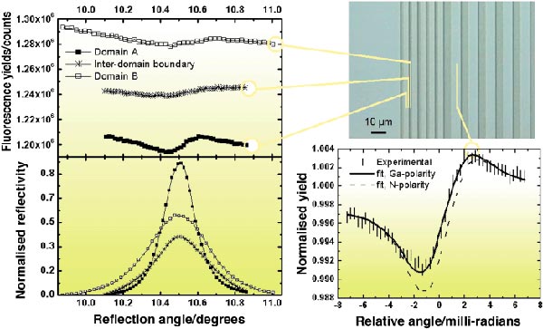
To prove the possibility of polarity determination on the microscopic scale we studied GaN thin films, which exhibit periodic domains of lateral polarity inversion with a periodicity of a few micrometres. The Ga polarity is achieved by the presence of a prior deposited AlN nucleation layer between the film and the Sapphire substrate. The thickness of the GaN-film was around 800 nm. We found these films being of relatively poor crystalline quality, with rocking curve widths between 0.5° and 1°, and with very low reflectivity of about 1% or less (Figure 110). Because of this large angular acceptance we could replace the 1-dimensional focusing lens by a 2-dimensional focusing compound refractive lens [3] and thus reduce the focal spot to 10 µm horizontal by 1.5 µm vertical.
 |
|
Fig. 110: Micro-XSW on polarity inverted GaN thin films (upper right). Reflectivity and Ga-fluorescence yields for two adjacent domains and the boundary in-between are shown in the left graph. A fitted XSW curve is shown in the lower right. |
Micro-XSW scans were performed through adjoined polarity domains with a step size of 1.5 µm. From our data we can distinguish the two different polarity domains. The domains which have been grown on an AlN nucleation layer exhibit Ga-polarity. This finding is in agreement with XSW-measurements of large GaN films grown directly on sapphire, which have the opposite, i.e. have N-polarity.
References
[1] B.W. Batterman, Phys. Rev. 133, A759 (1964); B.W. Batterman, Phys. Rev. Lett. 22, 703 (1969).
[2] V.V. Aristov, M.V. Grigorev, S.M. Kuznetsov, L.G. Shabelnikov, V.A. Yunkin, M. Hoffmann, E. Voges, Opt. Comm. 177, 33 (2000).
[3] B. Lengeler, C. Schroer, J. Tümmler, B. Benner, M. Richwin, A. Snigirev, I. Snigireva, and M. Drakopoulos, J. Synchrotron Rad. 6, 1153 (1999).
Principal Publication and Authors
M. Drakopoulos (a), J. Zegenhagen (a), A. Snigirev (a), I. Snigireva (a), M. Hauser (b), K. Eberl (b), V. Aristov (c), L. Shabelnikov (c), and V. Yunkin (c), Appl. Phys. Lett. 81, 2279 (2002).
(a) ESRF
(b) Max-Planck-Institut für Festkörperforschung, Stuttgart (Germany)
(c) Institute for Microelectronics Technology RAS, Chernogolovka (Russia)


