- Home
- Users & Science
- Scientific Documentation
- ESRF Highlights
- ESRF Highlights 2003
- X-ray Imaging
- Manganese K-edge X-ray Absorption in Highly Mn-doped GaN with Micrometre Resolution
Manganese K-edge X-ray Absorption in Highly Mn-doped GaN with Micrometre Resolution
Conventional electronic devices rely on the transport of electrons in a semiconductor such as silicon. Nowadays, however, the spin of the electron rather than its charge is being exploited to create a new generation of spintronic devices which will be smaller, more versatile and more robust than those currently making up silicon chips and circuit elements. Since Dietl et al. predicted that GaN doped with ~ 5 at.% of Mn should exhibit a Curie temperature exceeding room temperature [1], there has been tremendous advances on both the realisation of high-quality (Ga,Mn)N and on the theory of ferromagnetism in these spin-based semiconductors. However, one of the key unanswered question is whether the resulting material is indeed an alloy of (Ga, Mn)N or whether it remains as GaN with clusters, precipitates or second phases that are responsible for the magnetic properties.
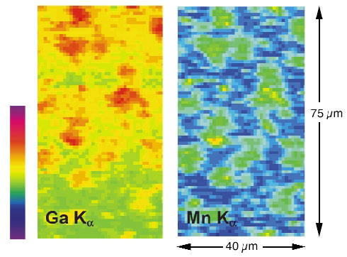
Therefore, in the present report elemental maps of Mn and Ga were taken at ID22 (beam size 1x1 mm2, photon flux ~ 5 x 10¹⁰ ph/s at Mn K-edge) on molecular-beam-epitaxy grown GaN:Mn layers deposited with Mn concentrations ranging from 1018 up to 1021 cm3. Uniform patterns with no intensity changes are observed for most of them, showing a homogeneous distribution of both elements at the length scale of the beam size. However, for the highest Mn concentration (5.4 x 1021 cm3), in addition to a visible roughness, Figure 143 reveals a close correlation between the Mn and Ga location confirming that there is a partial substitution of Ga by Mn [2]. It is also clear that the Mn atoms are somewhat interrelated among themselves, and they are not randomly distributed in the GaN lattice. Possibly at higher Mn level, local strain fields energetically favour the formation of Mn clusters by a mechanism similar to that of self-assembled growth of strained quantum dots. Because the surface atom diffusion length and the local strain field are both finite, Mn clustering would become more probable for strongly doped layers.
 |
|
Fig. 143: Ga and Mn maps of the highest Mn doped GaN sample obtained by measuring their Ka line intensities. The pixel size is 1x1 mm2. Red colour indicates high fluorescence intensity, blue colour low intensity. |
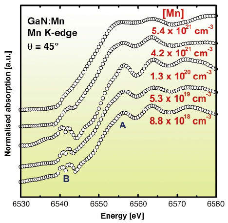
Figure 144 displays the Mn K-edge XANES data recorded at an incident angle ![]() = 45 ± 5°. We attribute the main feature (A) to dipole-allowed transitions of photoelectrons from Mn 1s states to unoccupied 4p-like states. Usually, the large density of unfilled d states from the transition metal do not contribute to a K edge, but in the absence of inversion symmetry mixing of the Mn 3d with N 2p character states from the surrounding atoms takes place [3], giving rise to the pre-edge peaks (B). The substitutional incorporation of a transition metal generally increases linearly the intensity of this pre-edge structure, showing a progressive participation of 3d orbital in the bonding. However, this strong hybridisation is not observed. The clear smoothing and broadening in the relative amplitude of all the distinguishable oscillation features reflects a change in the local chemical and crystallographic environment around manganese, supporting strongly the presence of doping-induced short-range disorder at very high manganese levels. This tendency is consistent with photoluminescence and Raman results. The higher Mn concentrated samples present a bound exciton transition less pronounced and more broadened, with a displacement towards lower energies. In good agreement, Raman frequency shifts of the corresponding E2 phonon mode confirm the doping-induced tensile strain in the GaN layers. No evidence of additional secondary phases and/or disorder activated phonon modes were observed, supporting that the long-range order was retained.
= 45 ± 5°. We attribute the main feature (A) to dipole-allowed transitions of photoelectrons from Mn 1s states to unoccupied 4p-like states. Usually, the large density of unfilled d states from the transition metal do not contribute to a K edge, but in the absence of inversion symmetry mixing of the Mn 3d with N 2p character states from the surrounding atoms takes place [3], giving rise to the pre-edge peaks (B). The substitutional incorporation of a transition metal generally increases linearly the intensity of this pre-edge structure, showing a progressive participation of 3d orbital in the bonding. However, this strong hybridisation is not observed. The clear smoothing and broadening in the relative amplitude of all the distinguishable oscillation features reflects a change in the local chemical and crystallographic environment around manganese, supporting strongly the presence of doping-induced short-range disorder at very high manganese levels. This tendency is consistent with photoluminescence and Raman results. The higher Mn concentrated samples present a bound exciton transition less pronounced and more broadened, with a displacement towards lower energies. In good agreement, Raman frequency shifts of the corresponding E2 phonon mode confirm the doping-induced tensile strain in the GaN layers. No evidence of additional secondary phases and/or disorder activated phonon modes were observed, supporting that the long-range order was retained.
 |
|
Fig. 144: XANES spectra as a function of the Mn content. |
In summary, scanning m-XRF shows the cluster formation on the micrometre scale for highly-doped GaN ([Mn] ~ 5.4 x 1021 cm3), while the incorporation of doping-induced defects, which clearly lower the short-range symmetry of GaN, was detected by XANES.
References
[1] T. Dietl, H. Ohno, F. Matsukara, J. Cibert, D. Ferrand, Science, 287, 1019-1022 (2000).
[2] M. Sato, H. Tanida, K. kato, T. Sasaki, Y. Yamamoto, S. Sonoda, S. Shimizu and H. Hori, Jpn. J. Appl. Phys. 41, 4513 (2002).
[3] F.W. Kutzler, C.R. Natoli, D.K. Misemer, S. Doniach, K.O. Hodgson, J. Chem. Phys., 73, 3274-3287 (1980).
Authors
G. Martínez-Criado (a), A. Somogyi (a), M. Hermann (b), M. Eickhoff (b), and M. Stutzmann (b)
(a) ESRF
(b) Walter Schottky Institute, Technical University Munich (Germany)


