- Home
- Users & Science
- Scientific Documentation
- ESRF Highlights
- ESRF Highlights 2006
- Materials Science
- New scientific opportunities at ID11
New scientific opportunities at ID11
Most materials occurring in nature such as rocks, ice and soil appear as complex heterogeneous and hierarchical aggregates of crystallites, domains and dislocation structures. Man-made materials from synthetic products to engineering materials are also usually polycrystalline and inhomogeneous, as are drugs and trace particles relevant to environmental matters as well as objects of artistic or archaeological significance. Furthermore, it is a general principle that many species with high chemical activity and/or interesting mechanical properties tend to be small grained and highly defective. Examples are metal hydrides, catalysts, battery materials, and nano-grained metals.
As materials science is a field in which we try to “bring the experiment to the sample”, rather than the inverse, our goal is to obtain high quality crystallographic and micro-structural data on even these defective samples. Ultimately, we aim to perform total simultaneous hierarchical characterisation (Figure 34) of arbitrary samples. To this end, we have developed an array of new diffraction-based methods based on high-energy microfocussing called three-dimensional X-ray diffraction (3DXRD) microscopy, to characterise polycrystalline samples over several length scales, from the Ångström scale (crystal structure) to the grain distribution over the entire sample (see [1] for a recent review).
 |
|
Fig. 34: Characterisation of a sample on several length scales: from the distribution of grains (left) to the crystal and molecular structures via 3DXRD. |
The sub-micrometre range is of particular interest in materials science as it is the critical length scale for many inter-granular interactions such as dislocations, cracks and interfaces; it is these interactions which ultimately give rise to the bulk properties of materials. The lack of a detailed knowledge of the distributional heterogeneity of properties on this scale has resulted in our inability to construct rigorous first-principles models of such basic materials properties as strength, fatigue resistance, and texture development. This length scale is also crucial in the microelectronics industry, where many features on modern chips are below 100 nm.
To study such features, bulk information may be collected by powder diffraction, but such data represents an ensemble average of the sample grains, and is uninformative on sample inhomogeneity, inter-granular interactions and the form of distributions of properties. Electron microscopy data has high spatial and angular resolution, but is limited to surfaces and static measurements. 3DXRD thus acts as the bulk equivalent of an electron microscope, acquiring spatial and structural data in the sub-micrometre scale in bulk samples in real time.
ID11 was one of first beamlines to open at the ESRF, and has been continually upgraded over the last ten years to take advantage of emerging technology and follow trends in materials science research. The development of 3DXRD on ID11 led to the construction of a dedicated station for high-energy microfocussing in the late 1990s. Due to the growing interest in these techniques, a new station has been built in order to extend this effort into the domain of high-energy nano-focussing. At the beginning of 2007, this outstation will become the first of the second wave of long beamlines at the ESRF open for the user programme.
With the present 3DXRD microscope, the spatial resolution is ~ 5 µm, while grains of 150 nm can be observed. The extension project aims to allow us to obtain sub-micrometre mapping resolution, with transverse resolutions below 100 nm and sensitivity to the earliest stages of nano-crystallisation. In order to achieve this, it will be necessary not only to obtain high-energy sub-micrometre beams, but also for the entire experimental configuration to be controlled on that length scale. The strong and ongoing optics development programme within the ESRF assures that several methods to produce sub-micrometre beams are available. Beam and sample position monitoring, and the integration with a feedback system, are the target of in-house development projects uniting several groups.
 |
|
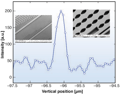
Fig. 35: 250 nm beam at 45 keV with nano-focussing silicon refractive lenses (inserts). Peak after deconvolution of knife-edge function. |
In the initial phase, focussing optics will consist of bent Laue crystals, a K-B multilayer mirror system, and a compound refractive lens “transfocator”, which allows tunable focus between about 1 µm and 1 mm by insertion of lenses in the beam. The smallest focus will be achieved by etched nano-lenses made with silicon wafer technology. During initial tests we have achieved 250 nm focus at 45 keV with this device (Figure 35) [2] and anticipate being able to achieve the design specifications of sub-100 nm focus at high (50 keV and greater) energy. Such high energy nano-focussed beams have never before been available, and should open up many exciting new experimental possibilities.
References
[1] D. Juul Jensen, E.M. Lauridsen, L. Margulies, H.F. Poulsen, S. Schmidt, H.O. Sørensen and G.B.M. Vaughan, Materials Today 9, 8-25 (2006).
[2] A. Snigirev, I. Snigireva, V. Yunkin, M. Grigoriev, S. Kuznetsov, G.B.M. Vaughan, M. Di Michiel, in preparation.
Authors
G.B.M. Vaughan (a), J.P. Wright (a), A. Bytchkov (a), C. Curfs (a), A. Snigirev (a), L. Margulies (a,b) and H.F. Poulsen (b).
(a) ESRF
(b) Risø National Lab. (Denmark)


