- Home
- Users & Science
- Scientific Documentation
- ESRF Highlights
- ESRF Highlights 2007
- X-ray Absorption and Magnetic Scattering
- Carrier doping by electric field effect in high critical temperature superconductors
Carrier doping by electric field effect in high critical temperature superconductors
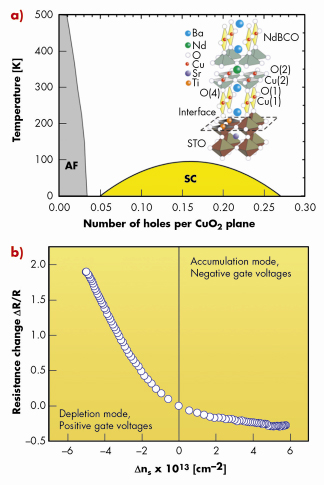
High critical temperature superconductor (HTS) physics is a subject of great interest that has led to much theoretical and experimental efforts. An intriguing point yet to be explained is the phenomenological T (temperature) vs doping phase-diagram (Figure 109a). Carriers are usually added to the 2D-CuO2 planes by chemical substitution in the adjacent charge-reservoir layers. For example, in the “123” family (e.g. Y1Ba2Cu3O7–![]() and Nd1Ba2Cu3O7–
and Nd1Ba2Cu3O7–![]() (NdBCO)), the oxygen content of the Cu(1)O chains in the charge-reservoir layer (see inset of Figure 109a) determines how many holes are transferred to the CuO2 sheets by a charge-transfer mechanism. Besides chemical doping, an elegant way to modify the number of carriers per CuO2 plane is to create a field effect device in which the channel is made of a very thin HTS film. The electric field creates charges (and therefore carriers) in the thin channel, and can modify the doping. Since HTSs are extremely sensitive to the number of holes present in the CuO2 planes, the electric field effect provides a very interesting reversible method to investigate the phase diagram. However, a direct doping of the CuO2 planes has not yet been demonstrated. A simple interpretation of the field effect mechanism, taken from the classical picture valid in Si/SiO2 MOSFET, fails in the case of the strongly electron-correlated HTS materials.
(NdBCO)), the oxygen content of the Cu(1)O chains in the charge-reservoir layer (see inset of Figure 109a) determines how many holes are transferred to the CuO2 sheets by a charge-transfer mechanism. Besides chemical doping, an elegant way to modify the number of carriers per CuO2 plane is to create a field effect device in which the channel is made of a very thin HTS film. The electric field creates charges (and therefore carriers) in the thin channel, and can modify the doping. Since HTSs are extremely sensitive to the number of holes present in the CuO2 planes, the electric field effect provides a very interesting reversible method to investigate the phase diagram. However, a direct doping of the CuO2 planes has not yet been demonstrated. A simple interpretation of the field effect mechanism, taken from the classical picture valid in Si/SiO2 MOSFET, fails in the case of the strongly electron-correlated HTS materials.
 |
|
Fig. 109: a) Phenomenological phase diagram of the cuprates and the structure of the NdBCO/STO interface studied in this work (inset). b) The change in the resistance of a 2 unit cell NdBCO film as a function of the injected holes by field effect. |
We studied the changes in the electronic states of Nd1.2Ba1.8Cu3O7 thin films under application of an electric field using X-ray absorption spectroscopy (XAS) at beamline ID08. The experiment was designed to measure the changes in both the XAS spectra and the conductivity of the device. A typical measurement of the change in the resistance as a function of the induced carrier density is shown in Figure 109b for an insulating 2 unit cell NdBCO film. As expected the channel resistance decreases from the hole depletion (negative gate voltage) to the hole accumulation (positive gate voltage) modes. A simple calculation of the expected change of carriers, based on the assumption that all the measured charges become carriers in the CuO2 planes, shows that a transition to the superconducting phase is expected. However, this does not occur.
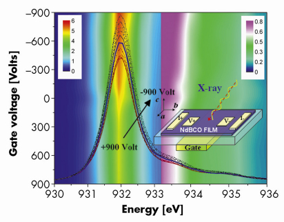
The reasons for this apparent discrepancy come from the XAS results. The effect of the electric field doping on the density of unoccupied states around the Cu L3 edge of a 3 unit cell is shown in Figure 110. Similar results were obtained on 2 unit cell (Mott insulating) and 4 unit cell (superconducting) samples. The Cu L2 spectra, measured on the NdBCO films at 10 K, present the typical features of all cuprates, i.e., a main peak at 932.0 eV and a shoulder at 933.5 eV due to the Zhang-Rice singlet [1]. The main changes occur around the main absorption peak at 932 eV, and are related to a doping of the Cu(1) ions in the chains of the charge reservoir [2]. The effect is strongly anisotropic, since the holes can be accommodated mainly in the ab plane, i.e. along the Cu(1)O chains. The increase of the Zhang-Rice satellite, reveals that a fraction of the holes is transferred to the conducting CuO2 planes. It is also worth noting that simultaneously the weight of the charge transfer peak (the satellite in the spectra) increases by the same amount, revealing that these carriers are transferred from the chains to the planes, doped by the field effect. This charge redistribution is necessary to reduce the build up of electrostatic energy.
 |
|
Fig. 110: Cu L3 edge total electron yield XAS spectra as a function of the gate voltage shown as colour maps around (a) the main 3d9 peak at 932 eV and (b) the Zhang Rice (3d9L ligand state) at 933.5 eV. Each XAS spectra measured at different gate voltages between +900 volt and –900 volt are overlapped to the colour map. A sketch of the experimental configuration used is shown in the inset. |
Our experiment demonstrates that the Zhang-Rice band occupancy, in turn related to the superconductivity, is changed by a field effect because of the charge redistribution between the CuO2 planes and the charge reservoir, and not by direct band-filling as in conventional band semiconductors and usually assumed to apply for HTS. This mechanism is the same governing the charge transfer from the chains to the CuO2 planes by chemical doping in the whole HTS family.
References
[1] M. Salluzzo, G. Ghiringhelli, N.B. Brookes, G.M. De Luca, F. Fracassi and R. Vaglio, Phys. Rev. B 75, 054519 (2007).
[2] G. Ghiringhelli, N.B. Brookes, C. Dallera, A. Tagliaferri, and L. Braicovich, Phys. Rev. B 76, 085116 (2007).
Principal publication and authors
M. Salluzzo (a), G. Ghiringhelli (b), J.C. Cezar (c), N.B. Brookes (c), G.M. De Luca (a), F. Fracassi (b) and R. Vaglio (a), Phys. Rev. Lett. (2008), accepted.
(a) CNR-INFM COHERENTIA and Dipartimento di Fisica Università di Napoli (Italy)
(b) CNR-INFM COHERENTIA and Dipartimento di Fisica, Politecnico di Milano (Italy)
(c) ESRF


