- Home
- News
- Spotlight on Science
- Submicrometre diffraction...
Submicrometre diffraction in dense arrays of three-dimensional germanium crystals
10-04-2012
Germanium grown epitaxially on micrometre-sized silicon pillars forms perfect crystals free of defects. The resulting Ge/Si “virtual substrate” is lighter and tougher than a free-standing Ge substrate and clears a path towards high-resolution CMOS X-ray detectors and high-efficiency multi-junction solar cells for both space and terrestrial applications. Submicrometre diffraction experiments at ID01 were used to analyse the tilt and elastic deformation of the pillars after the first micrometre of Ge deposition.
Share
While the world’s semiconductor industry is overwhelmingly focused on silicon (Si), the first solid-state transistor was made from germanium (Ge) in 1947. This material is returning to popularity thanks to its ability to extend and enhance the performance of Si-based electronics while remaining highly compatible with established fabrication plants. Current research focuses on nanometre-scale layers of Ge or SiGe alloys on Si substrates, for microelectronic [1] or optical applications [2], which exploit the quantum confinement of charge carriers.
Micrometre-scale layers of pure Ge are attractive for infra-red photodetectors, the final layer of triple-junction solar cells, or as “virtual substrates” for the deposition of GaAs-based layers. Increasing the Ge thickness still further (to several tens of micrometres) would enable the realisation of X-ray and particle detectors which are more efficient than their existing Si-based counterparts. The increased efficiency coupled with the good compatibility between Ge and Si leads to the final goal of a pixel detector in which the Ge absorbs the photons or particles and the resulting signals are handled by Si CMOS readout electronics.
The growth technique of low-energy plasma-enhanced chemical vapour deposition (LEPECVD) [3] has led to the efficient and fast deposition of such layers, but, once the Ge layer is more than a few micrometres thick, the thermal contraction during the cooling of the substrate back to room temperature after growth causes bending of the substrate and cracking of the Ge layer.
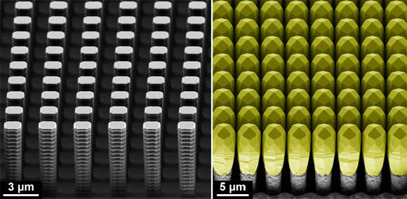
Growth of Ge on Si pillars (Figure 1) avoids the problem of bending and cracking on cooling. The Si substrate is patterned into micrometre-scale pillars using standard photolithographic and deep reactive ion etching techniques. During LEPECVD growth, Ge is deposited mainly on the tops of the silicon pillars due to the directionality of the flux of growth precursors onto the substrate and shadowing from neighbouring towers. Surprisingly, the Ge towers expand laterally until the space between them is just a few tens of nanometres, but they never coalesce. Very thick layers (up to 50 micrometres) can be grown, and the whole substrate is almost completely covered with closely-spaced towers. Cracking is completely avoided since each tower is free to elastically accommodate the strain induced by thermal contraction. Each tower could naturally form a single micrometre-sized pixel in a 2-dimensional X-ray CMOS camera.
Microdiffraction experiments carried out at beamline ID01 by a team of researchers from the ETH Zürich, Masaryk University Brno, and the L-NESS Politecnico di Milano, reveal the strain distribution within each pillar, and the tiny tilt angles between pillars.
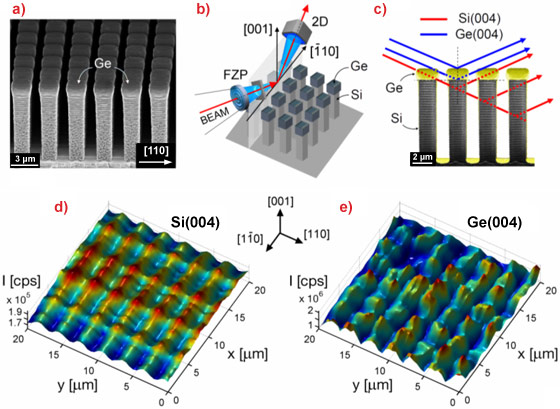
Silicon pillars were studied with only a 1 µm layer thickness of Ge (Figure 2a) on top, revealing the earliest stage of the growth and the distribution of elastic strain between the Ge and Si. The X-ray beam was focused onto a single tower using a Fresnel zone plate (FZP) in a wide-angle diffraction geometry (Figure 2b) in order to study the spacing and tilt of the crystalline lattice planes, with the diffracted signal collected by a 2-dimensional MAXIPIX pixel detector. However, signals from different pillars are mixed (Figure 2c) due to the shallow incidence angle. Intensity maps of the Si (Figure 2d) and Ge (Figure 2e) reflections allow the pillar positions to be identified. Full analysis of the synchrotron data is work in progress and expected to be published shortly.
While only the early stages of Ge growth have so far been studied at the ESRF, future experiments are proposed to study the structural quality of other semiconductors, such as GaAs, grown on Si pillars. GaAs is even more prone to cracking and defective growth when grown on flat Si wafers, but success here holds great promise for many applications in optical and photovoltaic devices such as light-emitting elements directly integrated with silicon electronics or high-efficiency solar cells on light and cheap Si substrates. In terms of the ESRF’s own interests, the X-ray detection applications are probably the most interesting. Arrays of Ge towers may form a new generation of X-ray pixel detector, finding application in many scientific fields at the ESRF itself.
Principal publication and authors
Scaling hetero-epitaxy from layers to three-dimensional crystals, C.V. Falub (a), H. von Känel (a), F. Isa (b), R. Bergamaschini (c), A. Marzegalli (c), D. Chrastina (b), G. Isella (b), E. Müller (d), P. Niedermann (e), and L. Miglio (c), Science 335, 1330 (2012).
(a) Laboratory for Solid State Physics, ETH Zürich (Switzerland)
(b) L-NESS, Department of Physics, Politecnico di Milano, Como (Italy)
(c) L-NESS, Department of Materials Science, Università di Milano-Bicocca, Milano (Italy)
(d) Electron Microscopy Center, ETH Zürich (Switzerland)
(e) Centre Suisse d’Electronique et Microtechnique, Neuchatel (Switzerland)
References
[1] B. Rössner, D. Chrastina, G. Isella, and H. von Känel. Appl. Phys. Lett. 84, 3058 (2004).
[2] P. Chaisakul, D. Marris-Morini, G. Isella, D. Chrastina, N. Izard, X. Le Roux, S. Edmond, J.-R. Coudevylle and L. Vivien, Appl. Phys. Lett. 99, 141106 (2011).
[3] C. Rosenblad, H. von Känel, M. Kummer, A. Dommann, and E. Müller, Appl. Phys. Lett. 76, 427 (2000).
Top image: Germanium crystals epitaxially grown on silicon pillars.


