- Home
- Industry
- Applications and case studies
- Electronics
Electronics
The electronics industry is constantly pushing the frontiers of research and innovation, with the goal to increase performances and energetic efficiency of devices, characterised by a constant trend to miniaturisation. The synchrotron source allows today to study devices at nanoscale, making it possible to characterise electronic materials with unprecedented spatial resolution. The mapping of electronic devices can be carried out with X-ray nano probes, through different techniques, namely nano- and micro-tomography, nano-diffraction, nano-fluorescence and FTIR microscopy, with a beam size that can range between 20 and 100 nanometers.
The ESRF can provide answers to the following challenges:
• Reliability and failure analysis: voids, precipitates, dislocations and delaminations on bulk devices and thin films.
• Stress and strain, mechanical properties: on single crystals, poly-crystals, thin films, epitaxial layers.
• Morphological and structural characterization: roughness, film thickness, 2D and 3D imaging, multimodal analysis.
• Microstructure: crystal orientation map and grain size distribution.
• Chemical analysis: composition, dopants, depth profiling, diffusion, contamination.
• Physico-chemical properties: magnetic, band structure, work function.
CASE STUDIES
Company or institute
CEA, in collaboration with STMicroelectronics and the Nanoelec Technological Research Institute.
Challenge
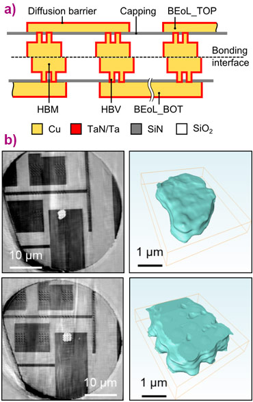
Researchers from CEA and STMicroelectronics and the Nanoelec Technological Research Institute have carried out an in-depth investigation of the specific reliability of interconnects produced through the hybrid bonding-based semiconductor integration process used in the construction of CMOS image sensors. They needed a non-destructive means to locate and measure voids formed within interconnects. Such voids are evidence of degradation caused by the electro-migration effect -- the migration of atoms driven by the electric current. The significance of this effect is compounded by the trend of reduction in structure size for more efficient microelectronics and its associated increase in current density.
Sample
A test vehicle was fabricated containing 100 linked back-end-of-line (BEoL) interconnects. These interconnects were formed by the direct bonding of two 300 mm-patterned wafers, with post bond anneal applied to strengthen the bonding. The bonded interface, the hybrid bonding metal (HBM), had a dimension of 3.6 microns and each HBM contained 16 hybrid bonding vias (HBVs). The electromigration test involved passing a current through the interconnects until a point of failure was reached, with the failure criterion set to a 10% increase in resistance (this value is indicative for the appearance of voids inactivating some of the HBVs).
Solution
Synchrotron-based X-ray phase-contrast nano-tomography at beamline ID16A was used to locate the voids formed during electromigration tests and to measure their volume. This technique avoided the complicated sample preparation necessary for other microscopy techniques and provided 3D information, which is generally preferable to address questions related to voids and porosity.
 |
|
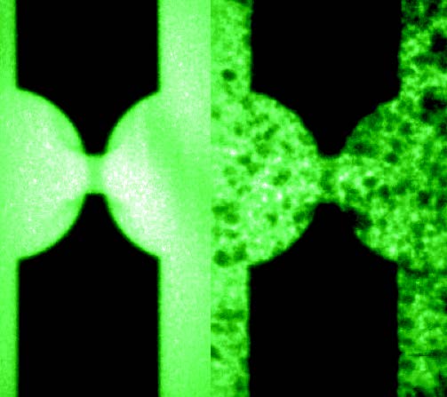
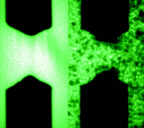
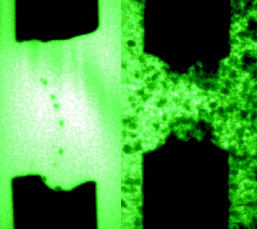
a) Schematic of the test structure showing its daisy-chain of interconnects. b) Illustrative tomography results after an electromigration test (350°C and 20 mA). Above and below, samples with the lowest and highest depleted volumes respectively. |
Benefits
Voids were localised only in the feed line (BEoL_TOP layer) above the via matrix on the anode side confirming that the type of hybrid bonding stack under investigation is immune to electromigration due to its constituent materials. Overall, the experiment demonstrated a linear relationship between electromigration induced void volumes and time-to-failure in hybrid bonding based test structures.
Reference
Correlation Between electromigration-related void volumes and time-to-failure by high resolution X-ray tomography and modeling, S. Moreau, A. Fraczkiewicz, D. Bouchu, P. Bleuet, P. Cloetens, J. Cesar Da Silva, H. Manzanarez, F. Lorut, and S. Lhostis, IEEE ELECTRON DEVICE LETTERS 40, 1808-1811 (2019); DOI: 10.1109/LED.2019.2945089.
Company
Mersen and SIMaP laboratory at the University of Grenoble
Challenge
Fuses can be found in most electrical circuits, where they protect electrical components against current surges. Despite their widespread use, however, nobody has ever watched what happens to a fuse as it explodes. With fuse breakdown typically taking place on timescales much less than a millisecond inside an opaque medium, in situ observations were thought impossible. Generating power from wind turbines and other intermittent sources relies on DC converters and fuses, but these tend to be bulky and complex compared to familiar AC versions. In DC circuits, the fuse has to manage current-interruption without profiting from the voltage passing through zero. Also, there is a big interest in reducing the dimension of the fuse because long fuses increase the inductance of the circuit, which is detrimental to DC inverters.
Solution
The SIMaP team used fast radiography with MHz frame rates on ID19 on commercial and test fuses to understand the interaction between electrical arcs and matter. The beamline allowed the team to measure the speed and lifetime of “burn-back” – an important process whereby the electrical arc damages the electrode material and creates silica cavities in the arc channel. Although previous post-mortem studies had shown various phenomena, they revealed little about the temporal characteristics of the process.
Benefit
Tracking the ultrafast processes that take place in fuses during electrical breakdown helped Mersen develop advanced compact fuses for renewable energy applications.
 |
 |
 |
| Breakdown of an electrical fuse at time intervals of 25, 100 and 500 microseconds (left to right) following a current spike, showing the effects of sand (right half of each panel) in the arc-quenching channel. | ||
Company
SILTRONIC (Germany)
Challenge
Silicon, the workhorse of the semiconductor industry is coming up against its physical limitations. To continue driving the increased speed, miniaturization and functionality of microelectronics, manufacturers are pairing silicon with other materials in order to enhance its properties. However, any imperfection in the microscopic structure of materials can severely affect the performance of the semiconductor devices. This is even more critical when matching two different materials.
Sample
SILTRONIC wanted to study the imperfections in silicon-germanium films on 300mm silicon wafers, a promising substrate for sub-20nm Complementary Metal-Oxide Semiconductor (CMOS) transistors (as used in computer microchips).
Solution
ID01’s scanning X-ray diffraction microscopy technique allows industrial researchers to detect the slightest imperfections in heterogeneous structures and thin films, even when stuck in different layers.
Benefits
The ESRF x-rays allowed SILTRONIC to establish a partial correlation between real-space morphology and structural properties of the sample at the micrometre scale. Results showed strain field fluctuations occurred due to the underlying dislocation network and that they diffused to the surface during growth.
 |
|
Siltronic's wafers. Credit: Siltronic. |
Company
University of Crete (Greece), Istituto di Struttura della Materia C.N.R. (Italy), ESRF
Challenge
Photovoltaic (PV) cells are mainly made of silicon, but organic polymer based PV cells offer a cheap and mass producible alternative with a low environmental impact. The efficiency of organic PV cells is poor and decreases markedly over time. So far they are not being used routinely in industry because they need to be able to harvest light more efficiently. Metallic nanoparticles added to the polymer layer allow localised surface plasmon resonances absorb light and promise high performance and durable solar cells.
Sample
Organic PV cells, made of a conjugated polymer and a soluble fullerene derivative.
Solution
X-ray diffraction and fluorescence spectroscopy at beamline ID11 provided characterisation of a multilayered organic electronic device coated with gold nanoparticles.
Benefit
Researches succeeded to detect changes in the nanoparticle distribution and structural properties of the organic layer, which will help enhance the efficiency of organic photovoltaic cells.
 |
|
Photovoltaic cells. |
partners


European Synchrotron Radiation Facility - 71, avenue des Martyrs, CS 40220, 38043 Grenoble Cedex 9, France.