- Home
- Users & Science
- Find a beamline
- Collaborating research group beamlines
- BM32 - IF - InterFace Beamline, French CRG
- BM 32 Featured Articles
- Self-Organized Growth of Nanoparticles on a Surface Patterned by a Buried Misfit Dislocation Network
Self-Organized Growth of Nanoparticles on a Surface Patterned by a Buried Misfit Dislocation Network
Self-Organized Growth of Nanoparticles on a Surface Patterned by a Buried Misfit Dislocation Network
F. Leroy, G. Renaud, A. Letoublon, R. Lazzari, M. Ducruet-Noblet
This page is under construction...
The fabrication of ordered metal and semiconductor nanoparticles on solid surfaces with uniform and controllable size and shape and with a high spatial density is an important challenge as it may find applications in future nanoelectronics, ultra-high density recording and nanocatalysis. The self-organized growth (SOG) of magnetic materials is an appealing technique for instance in view of magnetic recording.
We present here a new method based on a (001) metal surfaces nanostructured by a misfit dislocation network buried few nanometers below the surface. We show that the trapping energy of adatoms is large enough to allow an ordering of nanostructures at RT. The cobalt/silver interface is chosen because it is a test bed for magnetic nanoparticles, as Co exhibits a three-dimensional (3D) growth on Ag(001) and because it does not alloy at RT. To modulate the surface strain field, a Ag film was grown on a MgO(001) substrate. Due to the cube on cube epitaxial relationship and the 3% lattice mismatch between Ag and MgO(001), strain relaxation occurs via a square misfit dislocation network with a period of D~10 nm.
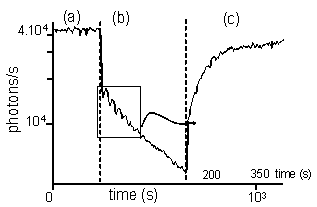
A 2D Ag film was first grown on MgO(001) at RT and then annealed at 900K, yielding a Ag(001) film of high crystalline quality, and exhibiting a well ordered interfacial DN as revealed by many diffraction satellites around the Ag Bragg peaks. Then the film was thinned in situ by ion bombardment until ~5 nm thickness (as determined by XR), while the thinning process was monitored by Ag(110) anti-Bragg GIXD measurements (Fig. 1). At 470 K (Fig 1.b) a layer by layer ablation mode was used to measure the thinning speed then the temperature was raised to 570 K (Fig 1.c) to stay in a regime of step retraction (Fig. 1c), thus keeping large terraces (100 nm) and low roughness.
 |
Fig.1: Ag(110) anti-Bragg peak intensity (logarithmic basis) versus time for different experimental conditions. (a) at 470 K before ion bombardment (IB) the intensity is steady. (b): IB is started and the temperature is kept at 470 K, the intensity decreases and oscillates, exhibiting a layer by layer ablation process (see inset). (c) keeping IB the temperature is increased up to 570 K: the intensity increases to reach a steady, maximum value. |
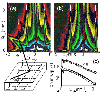
Before proceeding to the Co growth, a detailed (nano-) crystallographic study of the strain patterned substrate was performed by GISAXS. Similarly to GIXD experiments, this first step is necessary in order to analyze the GISAXS images which have been measured after Co deposition as interferences between the waves scattered by the substrate and those scattered by the Co nanostructures may occur. Figures 2(a) and (b) display two GISAXS images measured on the Ag/MgO(001) film with the incident X-ray beam respectively parallel to the <110> and <100> MgO(001) crystalline axes.
Sharp scattering rods in the direction reveal a periodic nanopattern of four-fold symmetry. As the intensity along the scattering rods quickly decreases as a function of , the GISAXS signal does not arise from a surface superstructure for which the intensity should be flat and extend much farther in . Therefore the measured rods are due to the buried DN. As expected, the in plane rod positions correspond to dislocation lines oriented along the <110> substrate directions, with a periodicity D=10.95 nm that matches to a coincidence site lattice of ƒ¼~37 oxygen atoms of the MgO(001) substrate and 38 (37+1) Ag atoms. The two scattering rods for the X-ray beam parallel to the <110> and <100> MgO(001) crystalline axes, are thus respectively labeled (1/ƒnƒ¼,1/ƒnƒ¼,L) and (2/ƒnƒ¼,0,L), using MgO(001) reciprocal lattice units.
 |
Fig. 2: (a) Experimental GISAXS pattern with the incident beam along the MgO[110] direction. The intensity is represented on a logarithmic scale and the Q// (resp. Q) axis ranges from –2 to 1 nm-1 (resp. 0 to 3.4 nm-1). The direct and reflected beams are hidden by a vertical beam-stop. The first order DN scattering rods are indicated by arrows. (b) Same as (a), but with the incident beam along [100]. (c) Scheme of the scattering geometry of GISAXS (d) Cuts along Q of the scattering rods of the dislocation network extracted from GISAXS pattern (a) (□) and (b) (○) (multiplied by 10 for clarity) and best fits of (solid lines), see eq. 1. |
The quality of the dislocation network is revealed by the correlation length of the superlattice, nm, as deduced from the Full Width Half Maximum ( ) of the scattering rods. A quantitative analysis of the (1/ƒnƒ¼,1/ƒnƒ¼,L) and (2/ƒnƒ¼,0,L) scattering rods was performed within the Distorted Wave Born Approximation (DWBA) framework since it provides a characterization of the dilatation field inside the Ag film and the MgO substrate, both parallel and perpendicular to the interface. As expected from the isotropic linear elasticity theory applied to a perfect misfit dislocation network, an exponential damping of the dilatation field as a function of the vertical z coordinate, was assumed inside the film and in the substrate, and the characteristic length of decay was found equal to 1.05 nm (Fig. 2d), as qualitatively expected.
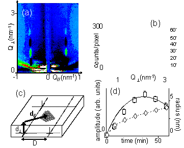
GISAXS measurements were then performed during the growth of Co on this nanostructured template for different substrate temperatures and Co growth rate. Co was finally deposited at room temperature and at a very low rate ( nm/min), respectively to decrease the thermal energy of the adatoms with respect to the DN nucleation trapping potential, and to increase the diffusion length of Co atoms and thus their probability to find a nucleation site. No ordering of Co clusters was found at higher temperatures or deposition rates. From the very beginning of the growth (0.04 nm), the subtracted GISAXS images (after and before Co deposition) display intensity oscillations along the DN scattering rods with a damped sinusoidal shape [19] (Fig. 3a). The oscillation amplitude increases with deposition time, reaches a maximum for an equivalent Co deposited thickness of 0.19 nm, and then decreases (Fig. 3b).
 |
Fig. 3: (a) Experimental interference pattern with the incident beam along the [110] direction, for a 0.14 nm-thick Co deposition (b) Intensity of the interference term versus Q, for different deposition times (symbols) with best fits (see text). Last (top) curve: interference term (circle) and best fit (solid line) for 0.14nm-thick Co deposition, and a simulated interference term (dashed line) for Co clusters located at the center of the unit cell. (c) Schematic representation of the Co clusters position with respect to the dislocation intersection lines (d) Oscillations amplitude versus time. Experimental data (□) and best fit (solid line) for the (1/,1/,L) DN rod as well as simulated curve of Co clusters radius versus time (short-dashed and ) for 2 AL high clusters. |
The period, equals to 5 nm, is a signature of the height difference between the Co clusters and the interfacial DN. Most importantly, these oscillations reveal the SOG of Co clusters, since an interference effect can only occur if the phase shift between the waves scattered by the Co clusters and those scattered by the DN is well defined, i.e. if the Co clusters are well localized with respect to the dislocations positions. Indeed, the intensity is the sum of three terms: the intensity scattered by the DN, the one scattered by the Co islands, and the interference term between both: (2) where FDN (resp. FCo) is the form factor of the DN (resp. the Co clusters), i.e. the Fourier transform of the dilatation field of the DN (resp. of the shape of the Co clusters), and and are the parallel and perpendicular coordinates of the Co clusters with respect to the dislocation crossing lines (Fig. 3c).
The very small intensity of the oscillations with respect to the rods before Co deposition (i.e. ) show that << . Hence, the term can be neglected in equation (2). Thus, the interference term, which contains the information on the Co clusters location, is simply obtained by the subtraction of GISAXS measurements after and before Co deposition. On the basis of the strain field symmetries, two high-symmetry sites are possible for the Co clusters: above the dislocation crossing lines or in-between. In order to discriminate between the two possible positions, the interference effect along the (1/ƒ¼,1/ƒnƒ¼,L) rod was simulated in the DWBA framework. The Co clusters were taken as cylinders whose height is an integer number of Co atomic layers (AL). The best fit was unambiguously obtained for the clusters located above the dislocation crossing lines (Fig. 3b), and a height of 2 AL.
To conclude, we have shown that the periodic surface strain field induced by a misfit dislocation network buried as far as 5 nm below a Ag(001) surface allows controlling the growth of Co clusters at RT, leading to self-organized growth. This result is supported by Molecular Dynamic simulations. We believe that this method could be used for many different systems, metal thin films being favored with respect to semiconductor ones because of the dislocation mobility necessary to reach the equilibrium state.
References
Phys. Rev. Lett., Fall 2005, in press


