- Home
- Users & Science
- Find a beamline
- Collaborating research group beamlines
- BM32 - IF - InterFace Beamline, French CRG
- BM 32 Featured Articles
- Study of wafer bonding interfaces
Study of wafer bonding interfaces
Study of wafer bonding interfaces with high energy X-rays (30 keV)
F. Rieutord, H. Moriceau, B. Bataillou, N. Sousbie
The study of solid-solid interfaces in the wafer bonding case is a typical case of the buried interface problem where the interface is now buried under typically 1mm of a dense solid (the silicon wafer). Very few techniques are available to compete with X-rays for that purpose as most classical surface study techniques (scanning probe, electrons etc...) interact too strongly to simply reach the interface.
 |
 |
|
Fig.1 Geometry of the interface X-ray reflectivity. The length of the material is adapted as a function of the absorption length of the material. For silicon at 30keV , it is typically 5mm. |
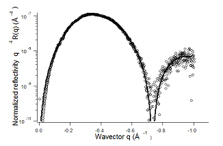
Fig. 2: Reflectivity curve of a hydrophobic bonding interface. Solid line is a fit to the data using a simple box model. |
In the present case we use (semi-) hard X-rays (30keV typically) to reduce absorption, combined with the use of grazing geometry to keep interface sensitivity. To study for example the interface between two materials A and B using X-ray reflectivity the geometry used is the shown in figure 1 where the X-ray beam enters the sample from the side and not from the top as in standard X-ray reflection.
Let us first consider the “textbook” example of what is referred to as “silicon hydrophobic bonding”, i.e. the bonding of two de-oxidized silicon wafer crystals (hence the crystal, being hydrogen passivated is “hydrophobic” as the contact angle with water is much larger than for clean oxide-covered wafers).
 |
 |
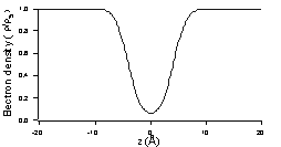
| Fig.3: Density profile corresponding to the fit of Fig.2. It corresponds to a rectangular box with rough sides, of width 9Å and a density at 0 close to 0. | Fig.4: Sketch of the two facing silicon surfaces at nanometer scale. The asperities from the two surfaces are compressed when the two wafers approach each other, resulting in a repulsion force that oppose attractive forces between the two solids. |
In this case, material A equals material B and in the case of a perfect bonding there would be no reflection coming out of the interface as there would be no electron density gradient. Hence any signal is the presence of a density change at the interface. The reflectivity curve of such bonding is shown in figure 2.
The curve shows in fact a very simple structure. A large hump which can be shown to be the first of a damped sinusoid extending to very high qs. Hence the density profile (fig 3) appears to be a simple rectangular box, with rough interfaces.
The surprising result in this case is that the depth of the electron density deficit at the interface is equal to the density of silicon, which shows that the space between the two wafers is essentially empty. The other surprising result of this very simple experiment is the distance between the two sides of the rectangular box, 9Å typically to be compared to the 2Å rms roughness of the silicon wafers.
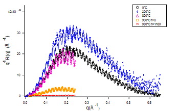
 Fig.6 Hydrophilic bonding reflection curves as a function of annealing temperature; note the increase of reflectivity between 0 and 200°C, due to water removal at the bonding interface, leading to an increased contrast.
The explanation for these results comes from rough solid adhesion models, transposed at the nanometer distance of silicon roughness. When the two surfaces come close to each other, the highest asperities get compressed (elastically or plastically) until they are numerous enough to bear the load (due e.g. to van der Waals attractive forces in this case).
Silicon being a rather stiff material, only a small number of asperities are sufficient to ensure the mechanical equilibrium. This can be quantified with a force balance.
The results obtained when including a statistical description of the interface together with van der Waals forces is in agreement with both the observed equilibrium distance and the magnitude of the pull-off force.
The technique has been applied also to the more technologically important hydrophilic bonding where two silicon oxide covered wafers are bonded together. The assembly results in an insulating silicon oxide film located in between two silicon crystals. If one of the wafer is thinned down, the technique can be used to obtained a Silicon-on-Insulator (SOI) substrates, an important component for the build-up of high speed, low voltage integrated circuits. In this case additional Silicon/Silicon oxide interfaces are visible that interferes with the signal issued from the bonding interface itself. This can be used to describe the whole profile and especially its temperature behavior. In this case, the gap between the wafers appears to be filled with water whose control upon annealing is a key point in hydrophilic bonding.
Interfacial X-ray reflectivity has also some peculiarities with respect to the X-ray data inversion. For example, with the x-ray beam entering from the sample side, it is possible to perform reflectivity experiments at positive or negative wavevector transfers. Also when used with two silicon wafers, there is no net index change crossing the interface and hence no critical angle on the reflection curve.
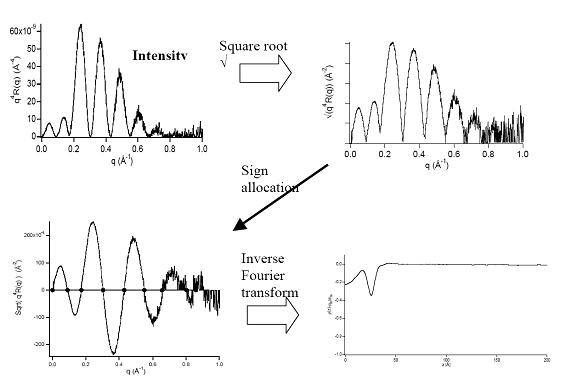
 Fig.7 Sketch of the inversion procedure in the case of a symmetric profile.. The phase problem reduce to a sign problem as the amplitude is now real. Sign change are visible as minima on the intensity curve.
An interesting case for data inversion is the case of symmetric bonding (i.e. the bonding of two identical material). As the electron density profile is symmetric its Fourier transform is real, the phase problem reduces to a mere sign problem. This possibility was used to perform direct inversion of the reflection data, with no uncertainties associated to the phase problem.
References
[1] F. RIEUTORD, H. MORICEAU, B. BATAILLOU, C. MORALES, and J. EYMERY, "X-ray characterization of bonding interfaces," presented at Semiconductor Wafer Bonding VIII: Science, Technology and Applications, Québec City, 2005.
[2] F. RIEUTORD, B. BATAILLOU, and H. MORICEAU, "Dynamics of a bonding front," Physical Review Letters, vol. 94, pp. 236101, 2005.
[3] H. MORICEAU, F. RIEUTORD, C. MORALES, S. SARTORI, and A. M. CHARVET, "Surface Plasma Activation before Direct Wafer Bonding: A short review and recent results," presented at Semiconductor Wafer Bonding VIII: Science, Technology and Applications, Québec City, 2005.
[4] H. MORICEAU, F. RIEUTORD, C. MORALES, A. M. CHARVET, O. RAYSSAC, B. BATAILLOU, F. FOURNEL, J. EYMERY, A. PASCALE, P. GENTILE, A. BAVARD, J. MÉZIÈRE, C. MALEVILLE, and B. ASPAR, "Direct Wafer Bonding for Nanostructure Preparations," 2005.
[5] H. MORICEAU, F. RIEUTORD, C. MORALES, and A. M. CHARVET, "Surface plasma treatments enabling low temperature direct bonding," Journal for Microsystem Technologies, 2004.
[6] F. RIEUTORD, J. EYMERY, O. PLANTEVIN, B. BATAILLOU, D. BUTTARD, and F. FOURNEL, "Investigations of buried Interfaces using high energy X-ray reflectivity," Materials Research Society Symposium Proceedings, vol. 678, pp. EE9.9.1, 2001.
[7] F. RIEUTORD, J. EYMERY, F. FOURNEL, D. BUTTARD, R. OESER, O. PLANTEVIN, H. MORICEAU, and B. ASPAR, "High Energy X-ray reflectivity of buried Interfaces created by wafer bonding," Phys. Rev.B, vol. 63, pp. 125408, 2001.
[8] H. MORICEAU, B. BATAILLOU, C. MORALES, A. M. CARTIER, and F. RIEUTORD, "Interest of a short plasma treatment to achieve Si-SiO2-SI bonded structure," presented at Semiconductor Wafer Bonding VII: Science, Technology, and Applications, 2003.
[9] D. BUTTARD, F. RIEUTORD, J. EYMERY, F. FOURNEL, and B. BATAILLOU, "Buried hydrophobic silicon bonding studied by high-energy x-ray reflectivity," Journal of Physics D: Applied Physics, vol. 36, pp. A205-A208, 2003.


