- Home
- Users & Science
- Find a beamline
- Collaborating research group beamlines
- BM32 - IF - InterFace Beamline, French CRG
- BM 32 Featured Articles
- Surface self-organization with buried dislocation
Surface self-organization with buried dislocation
Surface self-organization with buried dislocation networks by using Si hydrophobic molecular bondings
J. Eymery et al
To pursue the race to miniaturization of electronics, self-assembled configurations rather than artificially drawn structures are expected to play a major role in the design of nanometric devices. Many methods of self-assembling have been proposed ranging from epitaxy to colloïds but the majority of them suffer invariably from a statistical yield in the control of size and spatial position of the nanostructures. Our recent research has been focused to develop a way to control the lateral ordering of nanostructures at the wafer scale.
The lateral self-organization is obtained by the preferential patterning of a solid surface with local strain or morphology created by a periodic array of buried stressors. This array is formed artificially by the dislocations appearing at the interface of two clean identical silicon (001) crystals bonded with a crystallographic disorientation. Such hydrophobic bonding (without oxide) creates two dislocation networks according to the flexion and rotation angles of the two crystals: the first one is constituted of parallel mixed dislocation lines, whereas the second is a square network of screw dislocations.
 |
 |
|
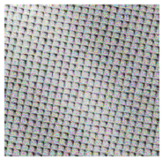
Fig.1: TEM image of a bonded sample in plane-view geometry (scale about 0.5x0.5 µm) with pure twist disorientation. The bonded-crystal thickness about 100 Å. |
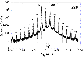
Fig.2: GIXRD Transverse scan along the (220) reflection the square dislocation network of Fig.1. The lateral period is 218 Å (about 1° of rotation). |
The general features of these arrays have been studied by Grazing Incidence X-Ray Diffraction (GIXRD) at the CRG/IF BM32 beamline at ESRF [1]. Fig. 1 shows an example of a TEM image of a square dislocation network and Fig. 2, its (220) GIXRD diffraction (i.e. the periodic lateral atomic-displacement) that can be modeled with kinematical calculations [2].
The propagation of the strain field through the bonded layer up to the surface, also measured by GIXRD rods, has been checked by continuum elasticity calculations [1]. Experimentally, thinning the bonded layer by sacrificial thermal oxidation to less than 10 nm increases the surface-strain. A clean and crystalline surface is then obtained after HF deoxidation. When two “twin” surfaces of Si(001) produced by the splitting of a single wafer are bonded together, we have only a relative in-plane rotation of the two crystal. For a small rotation angle, the periodicity of the network is inversely proportional to the rotation angle that can be controlled with a rotation angle of about 0.005° using an original patented method [3,4]. It is therefore possible to tune the periodicity of the dislocation network from few nanometers (<10° rotation) up to 2.2 µm (0.01° rotation). Moreover, by bonding twin surfaces at low rotation angle, there are almost no other defects at the interface, except some residual steps. To directly transfer the fourfold symmetry of the interface to the surface morphology, we use an etching solution consisting in a strain-dependent mixture of oxidant and deoxidant chemicals.
 |
 |
|
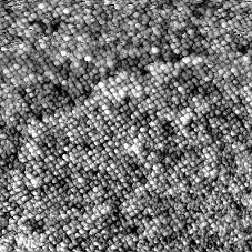
Fig.3. STM image of a patterned Si-surface (scale 1111 nm x 1111 nm). Nanostructures are 5 nm tall and separated by 25 nm. A residual step at the interface is observed closed to the diagonal line. |
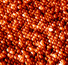
Fig. 4: STM image of the deposition of 9 Å of Ge at 490 °C on a patterned Si-surface (scale 555 nm x 555 nm). |
An example of nanopatterning of the Si surface is shown in Fig. 3 with a scanning tunneling microscope (STM) measurement. The patterning consists in a square array of silicon nanostructures, regularly spaced, with a lateral period of 25 nm consistent with the bonding angle of 0.88°, and peak-to-peak amplitude of about 5 nm. The bonded layer thickness is decreased from its initial value (110 nm) to less than 30 nm. The regularity of the buried dislocation network is preserved as indicated by GIXRD [5]. In this sample, the thinning procedure is obtained with a mixture of fluorhydric, nitric and acetic acid (so-called Dash-etch), and similar morphologies are reproduced with another solution (chromium oxide and fluorhydric acid). The bonding process and the chemical etching may be performed with full 300 mm wafers, so that this method is fully compatible with very large scale integration process.
 |
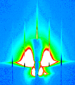 |
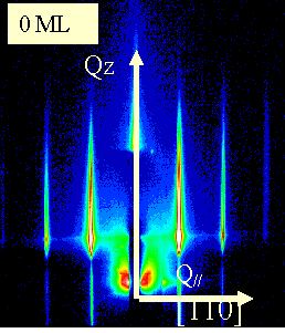
| Fig.5: GISAXS pattern of a surface similar to Fig. 3 (no Ge deposition, recorded using the SUV setup). The peaks correspond to the periodicity along the unit cell of the square dislocation network. | Fig. 6: GISAXS pattern recorded in SUV, after deposition of 15 ML of Ge, and substraction of the substrate image. Intensity oscillation on the rods and broad peaks signal are under analysis. |
The interest of this surface patterning is illustrated in Fig. 4 by growing 9 Å of germanium by molecular beam epitaxy at 490 °C (growth rate 0.7 Å/min) in the STM set-up [5]. A very original growth occurs with the localization of flat and rectangular Ge islands on top of the Si bumps, when the same deposition gives standard “hemispherical” islands (16 nm in diameter) on a flat substrate. This behaviour, quite unusual in the literature, may be explained by the Ge dots elastic relaxation due to the shape and size of the Si patterns. The example of Ge quantum dots growth on nanopatterned Si surfaces open the way to study the dependence in the nanometer scale of epitaxial deposition on the surface curvature and strain. Complementary experiments were performed using the SUV setup, which have been focused on the deconvolution of the Ge ordering signature from GIXRD and GISAXS patterns. Anomalous diffraction experiments and anomalous GISAXS (with image subtraction processing) are presently under analysis to quantify Ge dots positioning, strain and interdiffusion (M.I. Richard thesis with G. Renaud on the SUV setup). Examples of GISAXS patterns are shown in Figs. 5 and 6 for the initial surface and after deposition of 15 ML of Ge (i.e. quite a large amount compared to Fig. 4). The analysis was performed in situ (with GIXRD analysis) to measure the signal evolution during the deposition. Such templates are very convenient because the lateral periodicity and the depth of the patterns can be changed by varying the bonding or etching conditions. The pattern regularity is expected to narrow the size distribution, and therefore the physical properties of the nano-objects for deep enough nanostructurations. For the small corrugations, the coalescence of small Ge dots (that could be imposed by the network periodicity) to larger ones may occur in a way similar to flat surfaces.
Surface stress and morphology engineering by wafer bonding and chemical etching constitutes a general approach to assembly nano-materials in well-defined functional networks, with the high density required by applications. This approach is not resticted to semiconductor materials and is also potentially useful for organizing organic as well as non-organic nanostructures.
Reference
[1] J. Eymery et al., Phys. Rev. B 65, 165337 (2002).
[2] J. Eymery et al., Nucl. Inst. & Meth. B 200, 73 (2003).
[3] F. Fournel et al., Appl. Phys. Lett. 80, 793 (2002).
[4] K. Rousseau, J. Eymery, F. Fournel, J.P. Morniroli, J.L. Rouvière, Phil. Mag. 85 (21)(2005) 2415-2448.
[5] F. Leroy, J. Eymery, P. Gentile, and F. Fournel, Surf. Sci. 545 (2003) 211-219.
[6] F. Leroy, J. Eymery, P. Gentile, and F. Fournel, Appl. Phys. Lett. 80, 3078 (2002).


