- Home
- Users & Science
- Scientific Documentation
- ESRF Highlights
- ESRF Highlights 2001
- Applied and Industrial Research
- The "Lifetime" of Defects in Silicon after Ion-Implantation and Annealing
The "Lifetime" of Defects in Silicon after Ion-Implantation and Annealing
One of the major issues of concern for the future sub-micrometre integrated circuit technology is the fabrication of ultra-shallow junctions (< 100 nm) by dopant ion implantation in silicon at different energies ( 1 keV for B and some keV for As) and rapid thermal processing (RTP). These junctions will be necessary for the next CMOS technology nodes, where channel lengths of 0.13 µm in 2001 and 0.09 µm in 2004 are expected (International Technology Roadmap for Semiconductors, ITRS, 2000 update). In the last few years, leading companies have produced big efforts to construct innovative ion beamlines, in order to support this new frontier of ion implantation. Ion beams are now available with energies even below 1 keV and currents, high enough to ensure high wafer throughput for dopant ions of technological interest (boron, arsenic).
Lattice point defects and their agglomerates, introduced in silicon by the implantation process, play a crucial role in several processes used in the fabrication of electronic devices. Despite the immense technological interest in these defects, many of their properties are still unclear, due to the difficulty of determining the atomic configuration of complex cluster structures. The expected size of the defects induced by implants with keV energies and ion masses of B and As lies above that of simple point-like defects and below that of extended defects. Severe difficulties arise when the defect complexity increases and surface damaged layers of thickness of the order of 10 nm have to be investigated with conventional (laboratory) experimental techniques. Therefore, we have started an intense investigation by the technique of grazing incidence diffuse X-ray scattering (GIDXS) of the damage introduced into Si by ion implantation. GIDXS was chosen because of its high sensitivity to very shallow surface layers and to different atomic defect configurations.
 |
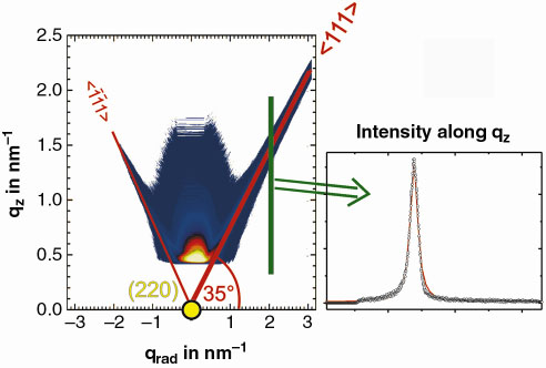
Fig. 155: GIDXS reciprocal space map of the intensity distribution close to the (220) surface reflection caused by extrinsic stacking faults on {111} planes. a) qz points along [001] and qradial along the [110] direction. The intensity along qz is measured by a PSD (green bar). |
The GIDXS has been developed and used on boron dopant atoms implanted in silicon at higher energies (35 keV). We have demonstrated the strength of the method to follow the defect transformation as a function of annealing treatments [1,2]. In essence, defect clusters consisting of B and Si interstitials of a diameter of about 4 nm are formed after implantation and low temperature annealing. After RTP the clusters dissolve and the corresponding diffuse intensity close to Bragg peaks (Huang scattering) decreases dramatically. The boron atoms become electrically active. The surplus silicon self-interstitials are condensed in extrinsic stacking faults on {111} planes, which produce characteristic intensity streaks along the <111> directions (Figure 155). The width of these streaks perpendicular to <111> is used to determine the size of the stacking faults, the integrated intensity is a measure of the number of self-interstitials bound in stacking faults. Depending on the temperature of the RTP, the kinetics of growth and dissolution of the stacking faults can be monitored by GIDXS as shown in the figure for the case of 1060°C. It is clearly demonstrated that within a short time-window of only 80 seconds the stacking faults grow and disappear almost completely (Figure 156).
 |
|
Fig. 156: Growth and dissolution of the extrinsic stacking faults as a function of annealing time at a RTP temperature of 1060°C (measurements performed at SSRL and ESRF). |
We have started a project called IMPULSE (Ion Implantation at Ultra-Low Energy for Future Semiconductor Devices), financed by the European Commission and involving scientists from five European institutions and a company in Germany. Due to the highly brilliant beam and the multi-circle diffractometer, beamline ID1 is ideally suited to the application of this promising technique for the first study of sub-keV energy implanted Si with dopants (B, As). The results obtained by GIDXS will be correlated with those of MEIS and TEM and with the depth profiles of the dopants measured by SIMS and SRP.
References
[1] U. Beck, T.H. Metzger, J. Peisl and J.R. Patel, Appl. Phys. Lett. 76, 2698, (2000).
[2] K. Nordlund, U. Beck, T.H. Metzger and J. Patel, Appl. Phys. Lett. 76, 846 (2000).
Authors
T.H. Metzger (a), M. Sztucki (a) and M. Servidori (b)
(a) ESRF
(b) LAMEL, Bologna (Italy)


