- Home
- Users & Science
- Scientific Documentation
- ESRF Highlights
- ESRF Highlights 2001
- Chemistry
- Structural Studies of Oriented Carbon Nanotubes
Structural Studies of Oriented Carbon Nanotubes
Carbon nanotubes have become a major research topic since their discovery in 1991 and offer many possibilities for future applications. The tubes consist of rolled up graphene sheets of sp2-bonded carbon atoms making a hexagonal network, and may be formed as single or multi-walled tubes. The inner diameters are typically in the one-nanometre range. Most structural studies have been made by direct imaging techniques but the use of diffraction techniques [1] is an important complementary method. The high-energy diffraction beamline ID15B is ideally suited to this type of investigation. Neutron diffraction measurements [2] have also been made.
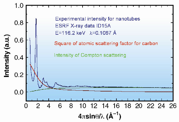
A typical diffraction pattern for a powder sample of multi-walled carbon nanotubes is shown in Figure 26. The first peak, 002, arises from the inter-layer spacing, which is a little larger than that for graphite. The other peaks show a characteristic asymmetric profile arising from the intra-layer correlations; the derived interference function can be transformed to give the pair correlation function. This spatial distribution gives detailed information of the atom positions in the graphene sheet and confirms the local graphitic order up to about 5 Å, but shows deviations at larger distances due to curvature and defects in the lattice. Carbon nanotubes fabricated by different processes exhibit a considerable variation in structure.
 |
| Fig. 26: X-ray scattering from a carbon nanotube sample [3]. |
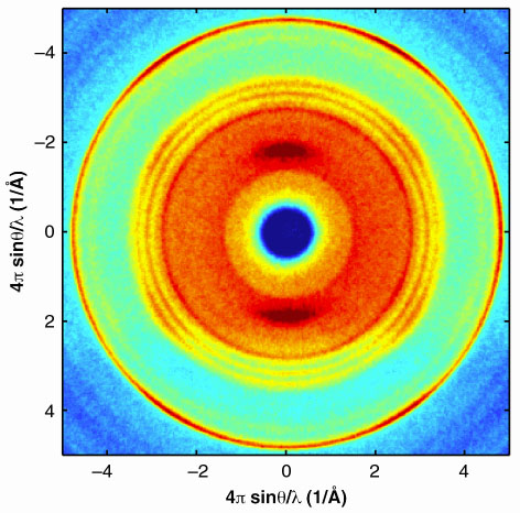
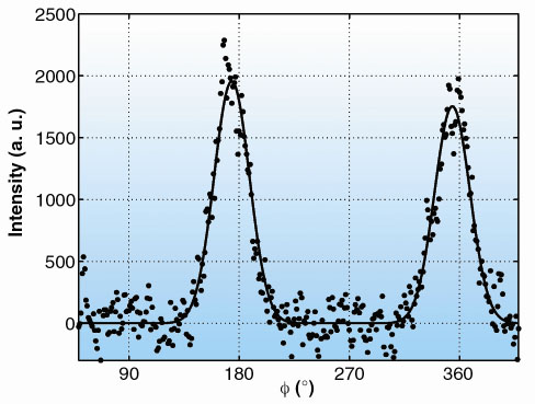
Oriented carbon nanotubes will be needed for the construction of electronic devices. This can possibly be achieved by the use of a microporous alumina template for the CVD process. A sample prepared by Kyotani [3] using this method has been studied on ID15B using the image plate detector to measure the anisotropic scattering distribution. When the membrane is oriented with the channels parallel to the beam direction, an isotropic scattering distribution is produced but if the membrane is positioned edge-on to the beam, the channels are perpendicular and there is an anisotropy in the 2D distribution, as shown in Figure 27. The dark spots correspond to the 002 reflection and give an indication of the alignment of the nanotubes; the azimuthal variation indicates a distribution with a half-width of approximately 17°. Other anisotropic features in the distribution have sixfold symmetry and seem to suggest reflections relating to the intra-plane structure. However, these features are the result of ordered alumina crystallites created during the CVD process that unexpectedly induces a phase transformation in the amorphous substrate.
 |
Fig. 27: The 2D intensity plot for scattering from carbon nanotubes in a templated alumina membrane |
The results confirm the partial alignment of the nanotube axes with the membrane channels. The full diffraction pattern also reveals the presence of defects in the nanotube structure compared with materials produced by other fabrication methods. Nevertheless, these initial studies have demonstrated the advantages of the high-energy diffraction method for these systems; a typical run corresponding to Figure 28 takes only 10 minutes. Further work is in progress.
 |
Fig. 28: The azimuthal variation of the diffraction intensity for the 002 peak of carbon (from Figure 27), showing the orientational dependence of the nanotube axes. |
References
[1] A. Burian, J.C. Dore, H.E. Fischer, V. Honkimaki, J.B. Nagy, T. Kyotani, J. Sloan and A. Szczygielska, Proc. 5th National Symposium of Synchrotron Radiation Users, Warsaw 1999, eds.: M. Lefeld-Sosnowska, J. Gronkowski, Warsaw University, 1999, p.7.
[1] J.C. Dore, A. Burian and S. Tomita, Acta Physica Polonica A, 98, 495 (2000).
[2] A. Burian, J.C. Dore, H.E. Fisher and J. Sloan, Phys Rev B, 59, 1665 (1999).
[3] T. Kyotani, L. Tsai and A. Tomita, Chem. Mater., 8, 2109(1996).
Principal Publication and Authors
J.C. Dore (a), A. Burian (b), T. Kyotani (c) and V. Honkimaki (d), in preparation.
(a) University of Kent, Canterbury (UK)
(b) University of Silesia, Katowice (Poland)
(c) Tohoku University, Tohoku (Japan)
(d) ESRF


