- Home
- Users & Science
- Scientific Documentation
- ESRF Highlights
- ESRF Highlights 2002
- Surface and Interface Science
- Structure of Ion-beam Synthesised SiC Nanocrystals in Si
Structure of Ion-beam Synthesised SiC Nanocrystals in Si
Due to certain physical properties SiC is regarded as a promising semiconductor material for micro- and optoelectronic devices at high temperature and high frequency, and for high-power applications. Thus, improvements of the growth processes are of great technical interest. SiC fabricated by ion-beam synthesis (IBS) can readily be integrated in the well-established Si technology. To this end the SiC crystallites must be confined to a thin surface or interface layer with an epitaxial orientation to the Si host lattice. IBS of SiC in Si is a complex multi-step process depending on the implantation conditions and the thermal treatment. In order to study a representative ensemble of SiC precipitates, various X-ray scattering techniques were used at the materials research station of beamline BM20 (ROBL-CRG) to reveal structural properties like shape, size and orientation distribution of the SiC nanocrystals.
 |
|
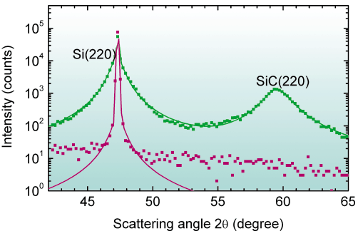
Fig. 37: Si(220) and ß-SiC(220) diffraction lines at grazing incidence and grazing exit for a Si wafer implanted with 3.25 x 1017 cm2 C ions of 45 keV at 500°C and post-annealed at 1200°C for 2 h. The X-rays penetrate 4 nm (magenta) or 1200 nm (green) into the material, respectively. |
Using grazing-incidence diffraction (GID) the Si (220) and ß-SiC (220) diffraction lines for a Si wafer implanted with C ions in a one-step process has been investigated. The radial scan is shown in Figure 37 for two incident angles. For a penetration depth of 4 nm (lower curve) only the Si(220) line from the perfect Si crystal surface layer is observed. If the radiation penetrates up to 1200 nm, additionally the ß-SiC (220) reflection is found, thus proving that the ß-SiC crystallites are located in the buried layer that was intended for the chosen deposition conditions. The analysis of the diffraction curves reveals the detailed structure of the SiC crystallites: the SiC(220) peak is shifted as compared to SiC values tabulated in the ICDD Powder Diffraction File, caused by the crystal lattice strain parallel to the surface. The line profile in the radial direction is influenced by the size of the SiC crystallites and by the strain fluctuation  d/d, while in angular scans (rocking curves) the line profile is governed by the SiC size and the orientation fluctuation (mosaicity)
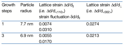
 . To extract all of these values, we used the tails of the Si(220) reflection, which can be considered as small-angle scattering from the holes in the Si perfect crystal filled with SiC crystallites (Babinet's principle). The line profile was fitted with a Lorentzian and gives the size of the SiC crystallites not superimposed by other properties. Table 1 shows results found for Si wafers implanted in one- and multi-step processes and post-annealed. The indices parallel and perpendicular distinguish the direction in the plane and perpendicular to the wafer surface. The orientation fluctuations (mosaicity) are < 1° for in-plane directions and in the range from 2° to 4° for the perpendicular direction. Within these limits the SiC nanocrystallites are aligned with respect to the Si host matrix.
 |
|
Table 1: Results of diffraction for Si wafers implanted in various steps with 3.25 x 1017 cm2 C ions of 45 keV at 500°C and post-annealed at 1200°C for 2 h. The particle size is determined from the Si(220) profile. The results for the parallel strain component are extracted from GID measurements on SiC(220) and for the perpendicular component from coplanar beam geometry they are within technically acceptable limits. |
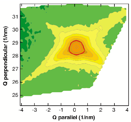
We also studied reciprocal space maps (RSM) of the ß-SiC (002) reflection in order to gain a complete two-dimensional characterisation of the implanted sample. Figure 38 shows such an RSM of material implanted with 4 x 1017 cm2 C ions of 195 keV at 800 °C (and no post-annealing). The adjacent, much stronger Si(004) reflection at Q|| = 0 nm1 and Q = 46.3 nm1 is located outside of the shown area. As the peak intensity of SiC is centred at the same Q|| value as the Si host lattice, and as the intensity distribution is narrow, one can conclude a very high degree of alignment of the ß-SiC crystallites. Furthermore, the streaks in the Si<111> directions indicate the growth of platelike (oblate) crystallites with facets extended in the {111} planes.
 |
|
Fig. 38: RSM of the SiC(002) reflection of crystallites formed by implantation of 4 x 1017 cm2 C ions of 195 keV into Si(001) at 800°C. The red line is the half maximum contour. |
By combining various X-ray scattering techniques (co-planar XRD, in-plane GID) on a versatile 6-circle diffractometer we are able to characterise IBS-manufactured buried SiC nanocrystal layers in Si standard wafers with regards to their depth distribution and their alignment with the Si matrix.
Principal Publication and Authors
F. Eichhorn (a), N. Schell (a, b), A. Mücklich (a), H. Metzger (c), W. Matz (a) and R. Kögler (a), J. Appl. Phys. 91, 1287 (2002).
(a) Forschungszentrum Rossendorf, Institute of Ion Beam Physics and Materials Research, Dresden (Germany)
(b) ROBL-CRG
(c) ESRF


