- Home
- Users & Science
- Scientific Documentation
- ESRF Highlights
- ESRF Highlights 2005
- X-ray Imaging and Optics
- Three-dimensional Imaging by Synchrotron Radiation Computed Laminography
Three-dimensional Imaging by Synchrotron Radiation Computed Laminography
Today, X-ray computed tomography – developed during the 1960s/70s for cross-sectional imaging in medicine – is an established technique at synchrotron sources for three-dimensional microimaging of materials and devices.
Computed tomography (CT) is optimised for samples whose (integral) X-ray transmission does not change significantly during rotational scanning, for example cylindrically-shaped samples undergoing rotation around their longitudinal axis. Despite the great success of CT for non-destructive imaging, it can be difficult to image the local microstructure within a limited region of interest when the sample size greatly exceeds the field of view of the detector. Indeed, inspection of devices such as flat, laterally extended microsystems on planar substrates by CT is often unsatisfactory since the strongly varying X-ray transmission during a scan is prone to generating artefacts.
This limitation has been overcome by introducing a new synchrotron imaging technique for 3D imaging of flat, laterally extended objects. This technique was stimulated by established laboratory methods from medicine (usually called digital tomosynthesis [1]) and non-destructive device testing (frequently called computed laminography [2]). These developments were carried out within an ESRF long-term project involving collaboration between the Fraunhofer IZFP, ANKA of Forschungszentrum Karlsruhe, the University of Karlsruhe and the ESRF.
Introducing a simple scanning geometry adapted to the particular experimental conditions of synchrotron imaging (such as the stationary source and parallel beam) allowed us to combine the advantages of laminography with those provided by synchrotron radiation. For instance monochromatic radiation was used to avoid beam hardening artefacts, high beam intensity permitted high spatial resolution and partial spatial coherence made it possible to exploit phase contrast.
Preliminary setups for data acquisition compatible with a stationary synchrotron source have been successfully implemented and tested at beamlines ID15 and ID19. The scanning geometry of synchrotron-radiation computed laminography (SR-CL) resembles that of SR-CT (see Figure 137) but the object rotation axis is inclined by an angle ![]() < 90 degrees with respect to the quasi-monochromatic X-ray beam incident from the multilayer monochromator. Contrary to (non-local) CT the lateral extension of the sample can be larger than the field of view of the area detector system.
< 90 degrees with respect to the quasi-monochromatic X-ray beam incident from the multilayer monochromator. Contrary to (non-local) CT the lateral extension of the sample can be larger than the field of view of the area detector system.
 |
|
Fig. 137: (a) Experimental setup sketched for SR-CL with monochromatic beam at beamline ID19; (b) The limiting case of the axis inclination angle |
In general for all laminography methods, the 3D Fourier domain is not sampled completely. Contrary to CT and depending on the exact scanning geometry (e.g. axis inclination angle ![]() ) there remain limited unsampled regions which could give rise to artefacts in the reconstructed images. The 3D reconstruction method, based on filtered backprojection adapted to the scanning geometry, minimises these artefacts.
) there remain limited unsampled regions which could give rise to artefacts in the reconstructed images. The 3D reconstruction method, based on filtered backprojection adapted to the scanning geometry, minimises these artefacts.
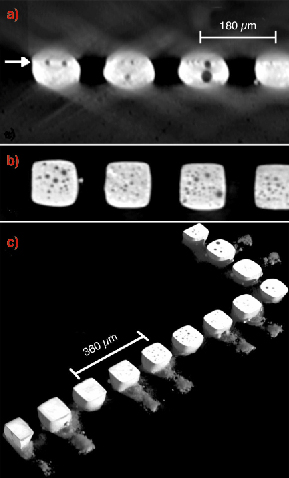
The capability of the method for non-destructive testing in microsystem technology was demonstrated using the example of a flip-chip bonded device. Solder bumps are hidden after the bonding process and thus are not accessible by visual inspection. Figure 138 shows two mutually perpendicular slices (a+b) through solder joints of the device, reconstructed from 900 projections with 1.4 µm pixel size taken at an X-ray energy of 35 keV. A variety of defects (small voids) which are located near the interface to the chip metallisations are related to the bonding technology and its processing parameters. In the 3D rendition (c) the chip itself is cropped by a slightly inclined plane in order to exhibit the square-shaped metallisations to the left-hand side and voids inside the bumps at the right-hand side. The large voids and solder splashes visible in the reconstructed image entail a reliability hazard of the electronic circuit.
 |
|
Fig. 138: Flip-chip bonded device: reconstructed cross-sections through a row of solder bumps, (a) perpendicular and (b) parallel to the device surface. The arrow in slice (a) indicates the depth position of slice (b) where many small voids are found. In the 3D rendition (c) the chip itself is cropped by a slightly inclined plane. Voxel size is 1.4 µm, X-ray energy 35 keV. |
The reported results demonstrate the feasibility of synchrotron-radiation computed laminography. A dedicated setup is scheduled for installation at ID19 in March 2006. SR-CL will then be readily applicable at the ESRF for non-destructive testing of flat, laterally-extended objects such as electronic components or flat samples of microstructured materials.
References
[1] J. T. Dobbins III and D. J. Godfrey, Phys. Med. Biol. 48, R65 (2003).
[2] J. Zhou, M. Maisl, H. Reiter, and W. Arnold, Appl. Phys. Lett. 68, 3500 (1996).
Principal Publication and Authors
L. Helfen (a,b), T. Baumbach (b,c), D. Kiel (b), P. Pernot (b,d), P. Mikulík (a,e), P. Cloetens (d), J. Baruchel (d), Appl. Phys. Lett. 86, 071915 (2005).
(a) Fraunhofer Institute for Nondestructive Testing (IZFP), Dresden (Germany)
(b) Institut für Synchrotronstrahlung (ISS/ANKA), Forschungszentrum Karlsruhe (Germany)
(c) Laboratorium zur Applikation der Synchrotronstrahlung, University of Karlsruhe (Germany)
(d) ESRF
(e) Now at: Institute of Condensed Matter Physics, Masaryk University, Brno (Czech Republic)


