- Home
- Users & Science
- Scientific Documentation
- ESRF Highlights
- ESRF Highlights 2006
- Surface and Interface Science
- Temperature influence on silicon nanodot pattern formation by ion-beam sputtering
Temperature influence on silicon nanodot pattern formation by ion-beam sputtering
The production of semiconductor nanostructures has awakened great interest due to their application in opto- and microelectronic devices. This has motivated intense research on new nanofabrication routes to further reduce feature size, which is of special importance for silicon due to its use in current semiconductor technology.
On the way to further miniaturisation, self-organisation methods are emerging as a promising approach, where nanoscale units are building-blocks that auto-assemble in meso- and macro-structures. Among these methods, ion beam sputtering (IBS), i.e. removal of atoms from the surface by ion impingement, has proven to be a competitive option for surface nanostructuring [1]. In a fast and convenient way, large areas of either metals, semiconductors or insulators, can be patterned in well-defined ways by choosing the proper IBS parameters. Typically, ripple or nanodot patterns are induced on semiconductor surfaces at off-normal and normal ion incidence, respectively. Theoretically, the formation of such patterns by IBS can be described from the balance between surface smoothening processes and an instability induced by the dependence of the sputtering yield on the local surface curvature.
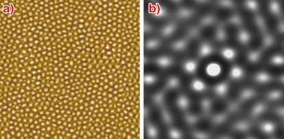
Among the relevant IBS parameters, temperature can play a significant role in the nanostructuring process by governing diffusion processes. In contrast with other variables, temperature has not been extensively studied experimentally in the case of IBS nanodot patterns. This has motivated our study of pattern formation on Si(001) surfaces. The patterns were produced by 1 keV Ar+ at normal incidence (for more details, see Ref. [2]) in the 300-625 K range and the resulting surface topography was imaged by atomic force microscopy (AFM) (Figure 82a). The nanodot pattern appears after some seconds (60-120s) of IBS for T < 525 K, and reaches a saturation state after a few minutes. The autocorrelation of the AFM images (Figure 82b) reveals short-range hexagonal ordering. As a result of the ion bombardment, a ~ 2 nm amorphous surface layer is induced [2].
 |
|
Fig. 82: a) AFM image (1x1 µm2) of a nanodot (height 6-7 nm) pattern produced by IBS on Si(001) surfaces after 10 min sputtering at 375 K; b) Autocorrelation image showing the hexagonal arrangement. |
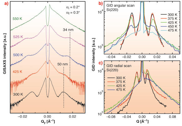
The patterns were further analysed with synchrotron light at the ESRF. The experiments were performed at the Anomalous Scattering Beamline (ID01) by using grazing incidence diffraction (GID) and small-angle X-ray scattering (GISAXS). These methods provide complementary information about the characteristic wavelength (interdot distance) and correlation length (ordered domain size), with additional hints about the relative contribution of the amorphous and crystalline volumes of the surface nanostructures. Radial GID scans are also sensitive to the presence of strain in the near surface region.
GISAXS and GID results from IBS patterns produced at different temperatures are displayed in Figure 83. The correlation peaks on both sides of the reflected and diffraction signal, respectively, are related to the pattern formation. The direct comparison of GID and GISAXS spectra shows that the nanodots are mostly crystalline at low temperatures (< 400 K). The correlation peak position gives the average inter-dot distance and the peak width is related to the degree of ordering. In contrast to theory, which predicts an increase of the pattern wavelength with temperature if thermal-diffusion dominates the smoothening mechanisms [3], AFM and X-ray methods reveal a decrease of the interdot distance (higher dot density). Also, the loss of correlation within the crystalline cores at 475 K indicates an increase of the amorphous volume with temperature which, in light of AFM data, can be understood by a progressive decrease of the dot height. Finally, there is an emerging strain near the surface (Figure 83c), which may affect diffusion processes. The former could explain the disagreement that has been found with theory.
 |
|
Fig. 83: GISAXS (a) and GID (b-c) scans. GID spectra were taken around the (220) in-plane Bragg peak in angular (b) and radial (c) directions. |
In conclusion, the synchrotron analysis has provided a deeper understanding of the pattern formation on Si(001) surfaces by IBS. Also, X-ray methods have given complementary information to local imaging techniques with better sampling statistics.
References
[1] U. Valbusa et al., J. Phys. Condens, Matter. C 14, 8153 (2002).
[2] R. Gago et al. Appl. Phys. Lett. 78, 3316 (2001).
[3] B. Kahng, H. Jeong, A.L. Barabasi, Appl. Phys. Lett. 78, 805 (2001).
Principal Publication and Authors
R. Gago (a), L. Vázquez (b), O. Plantevin (c,d), J.A. Sánchez-García (b), M. Varela (e), M.C. Ballesteros (e), J.M. Albella (b), and T.H. Metzger (d), Phys. Rev. B 73, 155414 (2006).
(a) Universidad Autónoma de Madrid (Spain)
(b) ICMM, CSIC, Madrid (Spain)
(c) CSNSM, Orsay (France)
(d) ESRF, Grenoble (France)
(e) Universidad Carlos III de Madrid (Spain)


